“Without data centers, GDP growth was 0.1% in the first half of 2025. Investment in “information-processing equipment and software” (which includes data-centers) represented about 4 % of U.S. GDP but accounted for ~92 % of GDP growth in the first half of 2025” /Harvard economist Jason Furman/
My tests show significant ability increases in reasoning for potential agentic work.
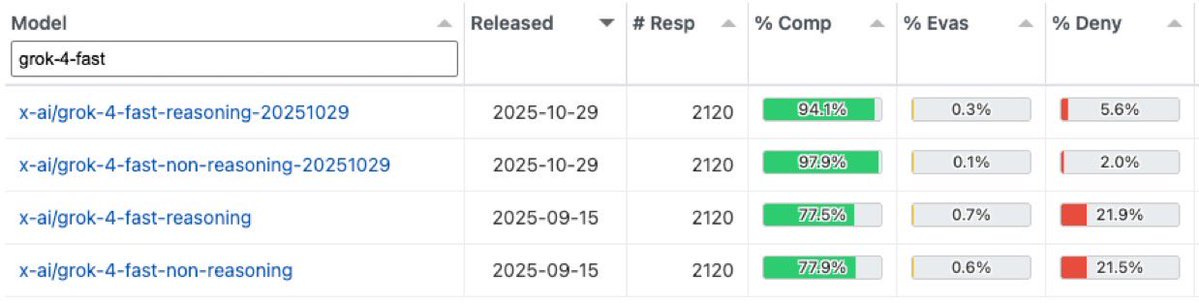
The fastest improving AI model in history… (Via @xlr8harder)
🙂
☑️ #111 Nov 8, 2025
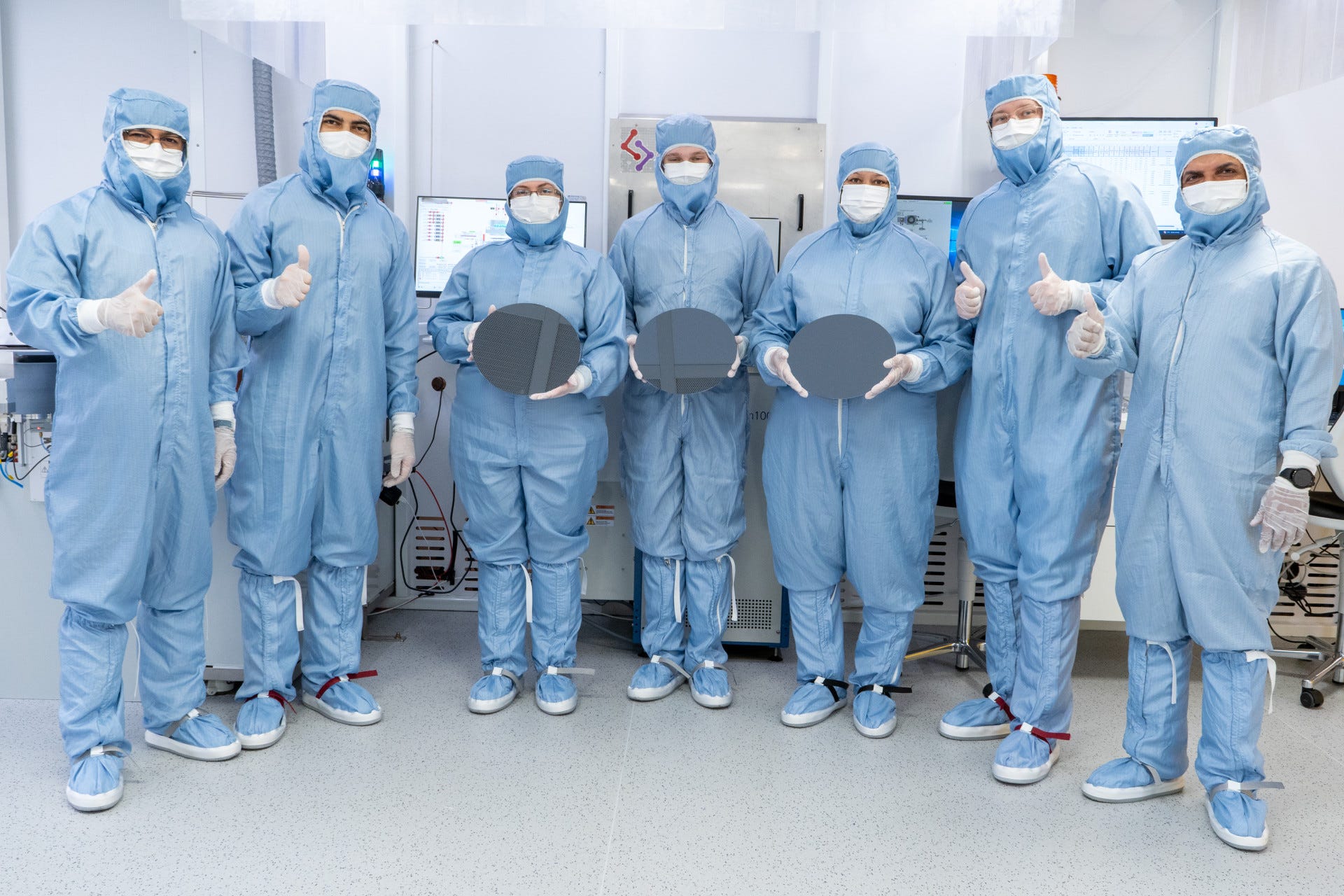
Semiconductors: The most important sector in the world
@ozeco: One of the most important article I’ve ever written, a collab with my friend @Strategist, is the most comprehensive deep dive you will ever find into semiconductors, the most important sector in the world, and it’s completely free!
Listen to the podcast or read the article to become an expert on semiconductors and understand the big trends from AI to semi production, fabless companies to equipment makers.
Have you ever wanted to understand:
How is the semi supply chain structured, why is it so globalized and what are the bottlenecks
What are the innovations at the heart of this space
How are chips made and who are the companies at the heart of this $600bn sector.
The fabless and foundry business models
The rise of China as a semiconductor giant
How the US is reshoring the semiconductor production with hundreds of billions of $
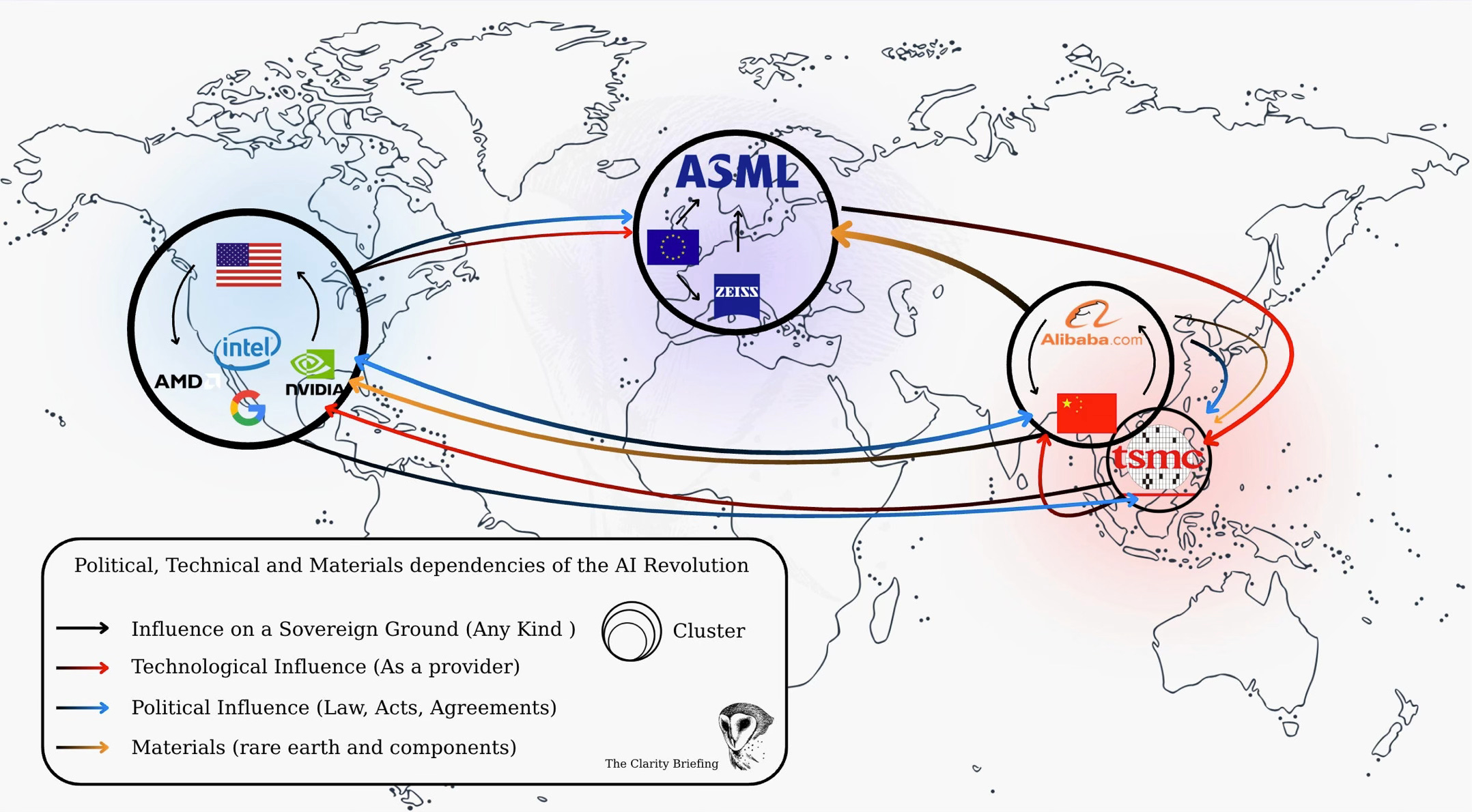
@claritybriefing: I tried to make the most understandable of current technological, material and political influence, map of the AI revolution.
Here’s how I see it:
The map shows three industrial cores and the forces that connect them. They influence each other through constraints: political, technological, or material. Each arrow reflects a specific dependency that shapes the AI economy.
United States → Europe
Political influence
The United States exerts political pressure on Europe through export regulations. Washington controls access to advanced GPUs, EDA software, and certain semiconductor technologies. Because ASML operates under Dutch jurisdiction but builds machines that use American components and intellectual property, the company falls under US export rules. When the US restricts China’s access to EUV or high-end DUV tools, Europe must align. This creates a one-directional dependency: Europe designs and builds the tools, but the United States decides who can receive them.
Mechanism: extraterritorial export law and licensing authority.
Effect: the US sets the boundaries of who Europe can sell advanced lithography to.
United States → Taiwan
Political influence
The US influences Taiwan’s semiconductor ecosystem through security guarantees, export controls, and strategic incentives. TSMC’s decision to build fabs in Arizona is a direct result of American political pressure combined with industrial subsidies. The US relies on TSMC for the most advanced logic chips, and it uses political tools to keep part of this capacity on American soil to reduce risk.
Mechanism: CHIPS Act incentives, security policy, export restrictions. Effect: TSMC expands in the US under strategic pressure, not pure economics.
Taiwan → United States
Technological influence
Taiwan holds the world’s most advanced manufacturing capability. Every major US tech company depends on TSMC’s nodes for performance: Nvidia, AMD, Apple, Google. The pace at which TSMC moves from one node to the next sets the ceiling for American AI growth. If TSMC slows, US compute slows.
Effect: US AI progress is gated by Taiwanese manufacturing.
Europe → Taiwan
Technological influence
Europe influences Taiwan through lithography. Without ASML’s EUV machines and Zeiss optics, TSMC cannot produce its leading-edge chips. This is not a symbolic dependency. It is physical and absolute. Every wafer that leaves TSMC’s 3 nm or 2 nm line carries ASML’s imprint.
Effect: Europe decides the pace at which Taiwan can advance nodes.
5. China → Europe
Material influence
China controls much of the global supply of critical materials used by European and Japanese semiconductor toolmakers: rare earths, gallium, germanium, high-purity chemicals. ASML, Zeiss, and the entire European optics chain depend on this upstream flow. Europe cannot cut China out without losing access to essential inputs for lithography production.
Mechanism: rare earth refining, chemical dominance.
Effect: Europe’s manufacturing capacity depends on Chinese materials.
6. China → Taiwan
Material and volume influence
China is both a major supplier of raw materials and a major consumer of chips. TSMC’s older nodes (28 nm, 16 nm, 7 nm) serve large Chinese customers. China also exports gases, wafers, and refined metals that feed into Taiwanese production. Even under sanctions, material interdependence remains high.
Effect: Taiwan’s fabrication ecosystem cannot fully detach from China.
7. United States → China
Political constraint
The direction of the arrow is not a flow but a block. The US limits China’s access to advanced GPUs, chip design software, and key lithography tools. This slows China’s ability to reach cutting-edge nodes and forces it to accelerate domestic alternatives.
Effect: China’s technological progress is constrained by US policy.
8. China → United States
Material influence
Despite political tension, the US remains dependent on China for a large portion of critical minerals and components. Even a fraction of disruption in Chinese supply chains can slow American manufacturing, data center construction, and chip packaging.
Mechanism: rare earths, graphite, minerals used in batteries and cooling systems.
Effect: Chinese materials underpin American hardware infrastructure.
The structural picture
The United States controls political levers.
Europe controls the lithography frontier.
Taiwan controls advanced manufacturing.
China controls the materials that feed the system.
No region is self-sufficient. Each holds one essential piece and lacks two others.
This is why the map looks like a triangle of constraints rather than an alliance network.
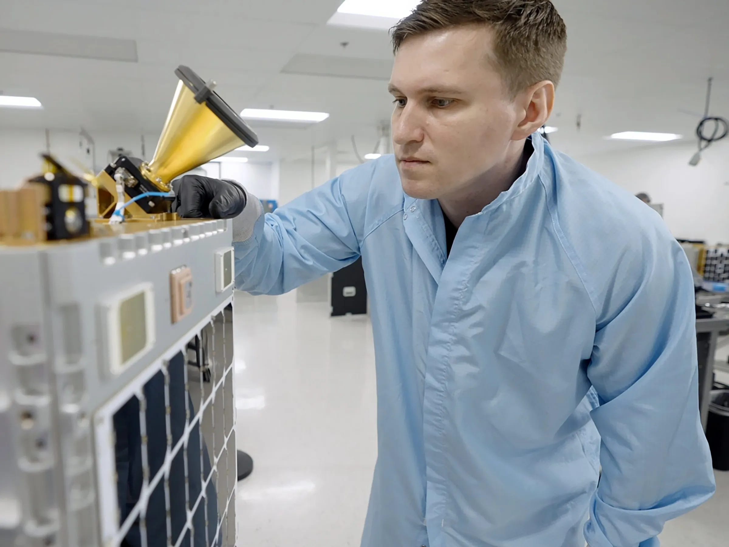
“The H-100 is about 100 times more powerful than any GPU computer that has been on orbit before,”
“It will be the first time that a terrestrial-grade data-center GPU will be flown and operated in orbit.”
Philip Johnston, CEO and cofounder of Starcloud, told IEEE Spectrum.
Starcloud cofounder and CEO Philip Johnston examines the star tracker, used for orienting a satellite carrying Nvidia’s GPU. Source: Starcloud, Inc. via IEEE Spectrum
“THE SINGULARITY IS NEAR: WHEN HUMANS TRANSCEND BIOLOGY”
@TOzgokmen: Which is these still companies exist today?
Why should NVDA have a 10-year lead?
Who knew about NVDA 10 years ago?
🙂
☑️ #106 Oct 29, 2025
American (and swedish) lithography
@OmerCheeema: I live in Eindhoven, the ASML town. I was chatting with an employee at a gym last night. He works on the mechanical engineering side of the wafer table for EUV machines. The job is to align wafers to the source and ready it for exposure. The alignment needs to be accurate at a micrometer level. And about 900 people at ASML work on it. Substrate, the startup, has 12 employees as seen on LinkedIn. ASML should offer them jobs.
<>
@BloombergTV: @BloombergTV: A secretive American startup says it has chipmaking technology to rival ASML and take on TSMC.
Bloomberg’s @EdLudlow breaks the story on Substrate’s particle accelerator-powered lithography machine and plans for an American foundry http://bloom.bg/48Q0LG7
news.bloomberglaw.com (10/28/25): [Excerpt] Thiel-Backed Chip Startup Is Seeking to Crack ASML Dominance (1) A secretive American startup has emerged with aspirations to challenge two titans of the semiconductor industry: ASML Holding NV and Taiwan Semiconductor Manufacturing Co.
The company, Substrate, has developed a new chipmaking machine that uses particle acceleration to handle lithography — the crucial process of etching microscopic circuitry onto silicon wafers. Claiming to have solved one of technology’s toughest problems, Substrate aims to compete with ASML, whose equipment is currently the only option for making advanced processors.
Substrate was founded to return the United States to dominance in semiconductor fabrication on three core beliefs:
The cost of semiconductor fabrication is out of control, and it will only continue to trend upward without radical new technological innovation
The United States is dangerously reliant on sources of geopolitical and supply chain risk that we do not directly control
The only chance the United States has to return to dominance in semiconductor production would be to create a new type of more vertically-integrated foundry, one that continues pushing Moore’s Law in both performance and cost
To achieve this, Substrate is building next-generation semiconductor fabs to return America to dominance in semiconductor production and will use our technology—a new form of advanced X-ray lithography—to power them.
Leading-edge semiconductor fabrication facility cost over time which follows a steady upward trend. Source: Substrate
linkedin.com: Atomic Layer Etching for Nano Device Fabrication
We provide an ALE-based method of manufacturing nanostructures with characteristic size below 20nm.
This is a new method of nanostructure fabrication using the atomic layer etching process, which is inherently a damage-free etch process. Owing to the etching process’s selectivity to inclined surfaces, which has been recently discovered, the inclined surfaces can be used as a mask and in this way walls of tapered structures, which can be readily fabricated by e.g., dry etching or epitaxial growth, will provide masking during the atomic layer etching process. This is why this process provides access to fabrication of extremely small structures in a very precise and efficient way.
alixlabs.com (10/7/25) [Excerpt] AlixLabs Secures Notice of Allowance for US Patent for Innovative Semiconductor Manufacturing Technology.
Lund, Sweden – October 7, 2025 – AlixLabs, a pioneering Swedish semiconductor equipment startup, today announced that the United States Patent and Trademark Office (USPTO) has issued a Notice of Allowance for the continuation of its internally named “Tetris” patent. The new patent strengthens and broadens AlixLabs’ intellectual property portfolio, covering key innovations in selective side wall masking technology that integrate self-aligned double patterning (SADP) with the company’s proprietary Atomic Layer Etching-based Pitch Splitting (APS™) process.
Source: AlixLabs AB
🙂
☑️ #105 Oct 18, 2025
Data (digital) tasks: new data wave
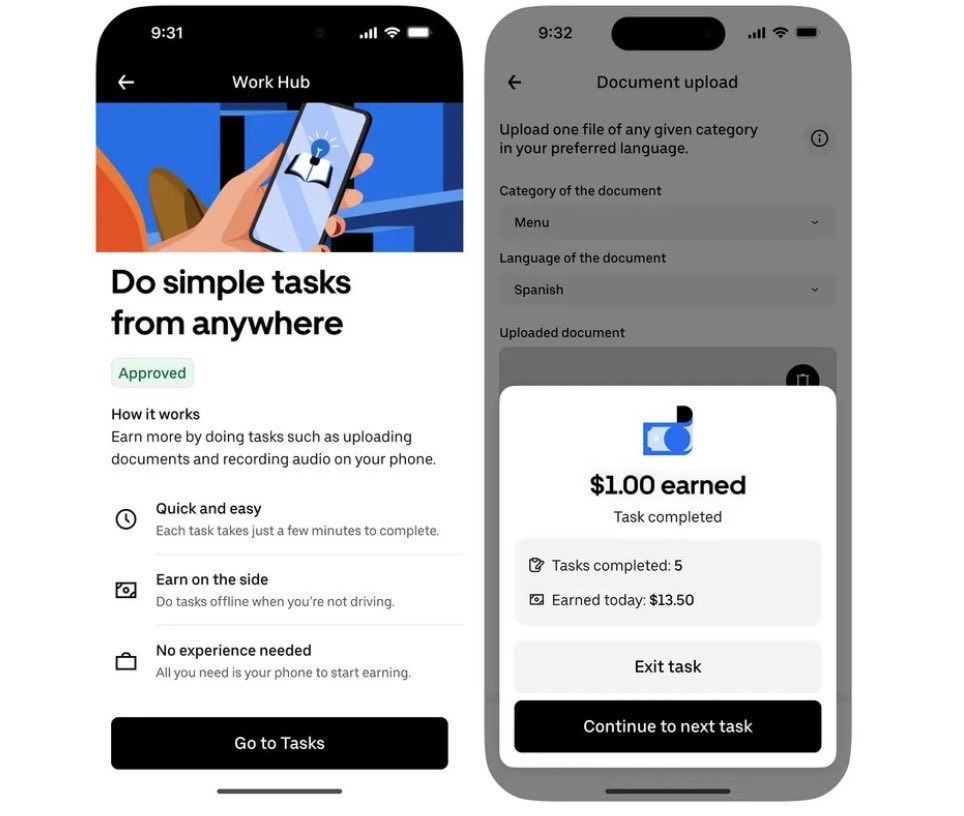
@bearlyai: Uber will give its drivers in the US an option to make money by doing “digital tasks”. These short minute-long tasks can be done anytime including while idling for passengers:
data-labelling (for AI training)
uploading restaurant menus
recording audio samples of themselves
narrating scenarios in different languages
The opportunity is quite larges based on fact that two AI data-labelling startups (Scale AI, Surge AI) each reached ~$30B valuations.
Earlier in October, Uber — which has 1m+ drivers in the US — had acquired Belgian data-labelling startup Segments AI for an undisclosed amount.
Scaling Compute as a Moat: Going from 0 to 200,000 GPUs in just over 200 days was practically unheard of. That puts xAI’s Colossus ahead of all but a few hyperscalers in terms of raw compute, making this infrastructure the central competitive moat for LLM training and inference at scale.
The core idea: Whoever owns (or controls) the most compute wins.
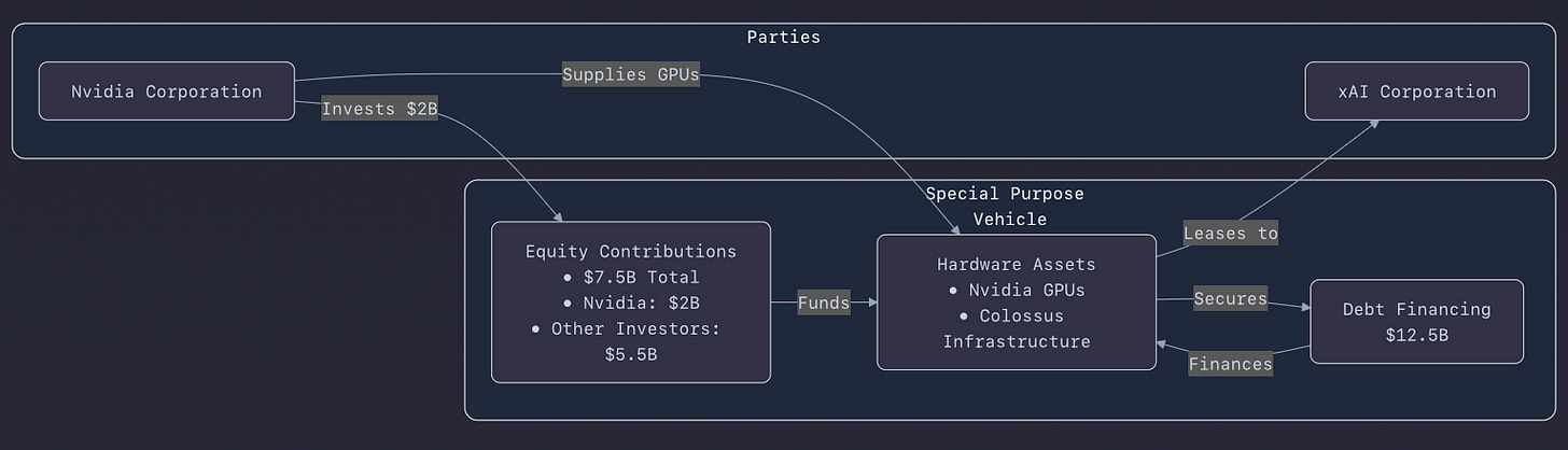
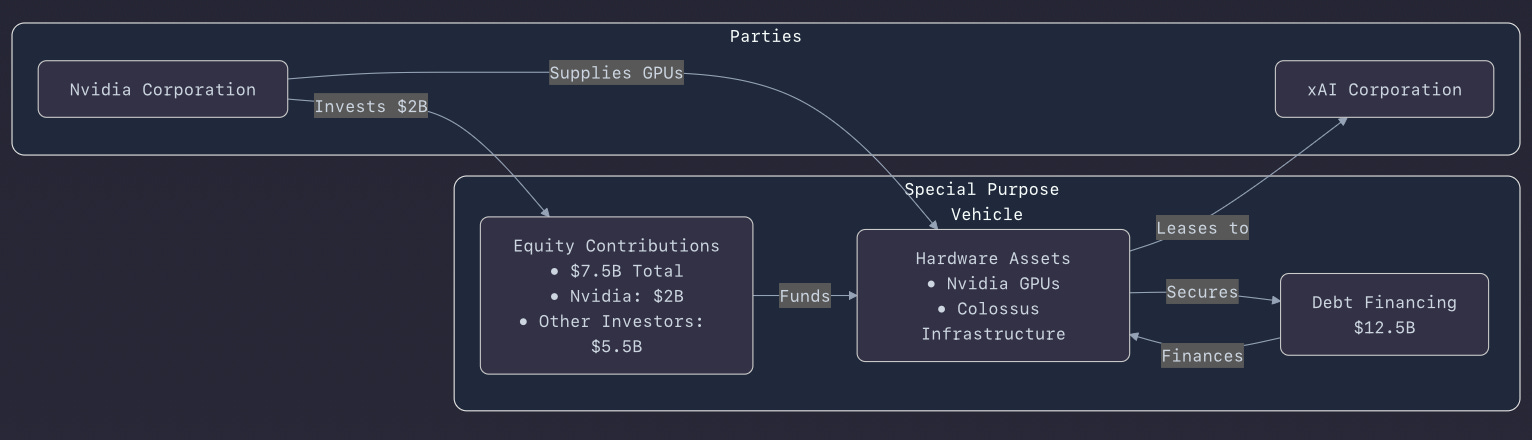
In only 122 days, xAI built its first huge data center, Colossus in Memphis, Tennessee, equipping it with 100,000 Nvidia GPUs. 92 days later, capacity was boosted to 200,000 units. Now, Antonio Gracias (Valor Equity Partners) anchors xAI Corporation’s plan to raise $20 billion for a deal using a special purpose vehicle (SPV) that would acquire semiconductors from Nvidia Corporation and then lease them to Colossus 2.
perplexity.ai and phind.com (Phind-70B) > [Sources not verified. Do your own research]: In the AI arms race, models matter—but scale, speed of iteration, and compute density are increasingly the differentiators. xAI clearly sees this and is making infrastructure its front line.
xAI’s rapid execution in scaling its compute infrastructure is one of the most striking industrial feats in recent tech history. Building and doubling capacity at Colossus in just over seven months illustrates the extreme speed and capital availability shaping the current AI arms race. A few key implications stand out:
Vertical coordination and financing: By using a special purpose vehicle (SPV) backed by Antonio Gracias and Valor Equity Partners, xAI is effectively separating asset ownership (semiconductors) from operational use (Colossus 2). This structure minimizes balance sheet strain while ensuring access to scarce Nvidia GPUs—an ingenious financial engineering move under today’s hardware constraints.
xAI’s infrastructure strategy for its “Colossus 2” data center in Memphis, Tennessee, represents a significant departure from traditional AI development. The initial “Colossus 1” site already boasts over 200,000 Nvidia H100 GPUs. For “Colossus 2,” the focus is shifting to even more advanced hardware, with plans for 550,000 Nvidia GB200 and GB300 GPUs, aiming for an eventual total of 1 million GPUs within the entire Colossus ecosystem. Elon Musk has publicly stated an audacious goal for xAI to deploy 50 million “H100 equivalent” AI GPUs within the next five years. This scale is unprecedented, requiring a “gigawatt-scale” facility – one of the largest, if not the largest, AI-focused data centers globally, with xAI constructing its own dedicated power plant, Stateline Power, in Mississippi, to supply over 1 gigawatt by 2027. (wral news)
phind.com: The financial breakdown is sourced fromn markets.financialcontent.com which mentions “$7.5 billion in new equity and up to $12.5 billion in debt.”
Strategic positioning vs. hyperscalers: This model could allow xAI to scale faster than Big Tech peers locked into more traditional data center expansion timelines. If successful, it may pioneer a new hybrid approach—AI companies as “GPU tenants” rather than infrastructure owners.
Market dynamics and geopolitical influence: The Memphis facility marks a strategic domestic placement, likely aligned with U.S. policy goals to repatriate critical computing capacity. It also signals Nvidia’s continuing dominance in AI training chips, though at the cost of creating systemic dependency between the two firms.
Capital and risk outlook: Raising $20 billion through a single-purpose leasing vehicle signals investor appetite is still robust for foundation-model infrastructure, but it raises questions about long-term ROI and operational leverage—especially as new architectures (custom ASICs, emerging competitors) evolve.
Overall, this move looks like a high-risk, high-return bet designed to secure xAI’s independence in compute supply while cementing its position as a world-scale AI developer. It shows Elon Musk’s consistent playbook: integrate critical capabilities early and finance with partners willing to think in decades, not quarters.
Elon Musk’s artificial intelligence startup xAI is raising more financing than initially planned, tapping backers including Nvidia to lift its ongoing funding round to $20 billion, according to people familiar with the matter. Nvidia is investing as much as $2 billion in the equity portion of the transaction, the people said. Bloomberg’s Annabelle Droulers reports.
PrateekJ17 (10/12/25): So we started this because we needed a way to provision infrastructure for AI agents at scale. Turns out nobody had really solved this properly. We wanted agents that could just... spin up a VM when they needed one, do their thing, and shut down. Simple idea, but getting it to actually work reliably was a whole journey. What we ended up building:
Agents that can deploy and control their own virtual machines An orchestration layer that doesn’t fall over when you scale to 100+ agents Support for pretty much any LLM (GPT-5, Claude, local models, whatever) Real monitoring because debugging invisible agents is a nightmare
The whole thing is open source. Apache license. No strings attached. We’re using it for automated testing and web scraping stuff, but honestly people are probably going to use it for things we haven’t even thought of. If you’ve ever tried to run computer-use agents in production, you know the pain points. That’s what we tried to fix. GitHub: https://github.com/LLmHub-dev/open-computer-use
PrateekJ17 (10/14/25): We open-sourced XAI’s Macrohard, an autonomous computer-using agent.
Sustainable and adaptive Scake Data Centers and Builld-to-Scale solutions for global hyperscale, AI/HPC, and enterprise customers
aligneddc.com: [Excerpt] AIP was founded by BlackRock, Global Infrastructure Partners (GIP), a part of BlackRock, MGX, Microsoft, and NVIDIA to expand capacity of AI infrastructure and help shape the future of AI-driven economic growth. Its financial anchor investors include the Kuwait Investment Authority and Temasek.
In less than a decade, Aligned has evolved into one of the largest and fastest growing data center companies globally. The Company designs, builds, and operates cutting-edge data campuses and data centers for the world’s premier hyperscalers, neocloud, and enterprise innovators. Aligned’s portfolio includes 50 campuses and more than 5 gigawatts of operational and planned capacity, including assets under development, primarily located in key Tier I digital gateway regions across the U.S. and Latin America including Northern Virginia, Chicago, Dallas, Ohio, Phoenix, Salt Lake City, Sao Paulo (Brazil), Queretaro (Mexico), and Santiago (Chile).
Beginning in calendar Q3 2026, Oracle will be the first hyperscaler to offer a publicly available AI supercluster powered by 50,000 AMD Instinct MI450 Series GPUs
oracle.com: [Excerpt] Oracle and AMD Expand Partnership to Help Customers Achieve Next-Generation AI Scale.
AMD Instinct MI450 Series GPUs Coming to OCI
AMD Instinct MI450 Series GPU-powered shapes are designed to deliver high-performance, flexible cloud deployment options and provide extensive open-source support. This provides the ideal foundation for customers running today’s most advanced language models, generative AI, and high-performance computing workloads. With AMD Instinct MI450 Series GPUs on OCI, customers will be able to benefit from:
Breakthrough compute and memory.
AMD optimized “Helios” rack design.
Powerful head node.
DPU-accelerated converged networking.
Scale-out networking for AI.
Innovative UALink and UALoE fabric.
Open-source AMD ROCm™ software stack.
Advanced partitioning and virtualization.
To give customers that build, train, and inference AI at scale more choice, OCI also announced the general availability of OCI Compute with AMD Instinct MI355X GPUs. These will be available in the zettascale OCI Supercluster that can scale to 131,072 GPUs. AMD Instinct MI355X-powered shapes are designed with superior value, cloud flexibility, and open-source compatibility. Learn more here and here.
chat.openai.com: [Sources not verified. Do your own research] Key Specifications & Architecture
The MI450 Series are AMD’s next‑generation data center / AI training & inference GPUs, built on CDNA “Next” architecture (sometimes referred to CDNA 5 in reporting). They will be manufactured using TSMC’s 2 nm (N2) process technology, which gives performance/power/density advantages over previous nodes. (Datacenter Dynamics)
AMD is positioning variants within the MI400 family: for example, MI450X, aimed at large‑scale AI workloads (low‑precision / inference), and MI430X, for HPC/high‑precision workloads (FP32/FP64). These variants will have differentiated logic (dropping certain precision units in each to optimize die space).
The MI450X is expected to lean heavily on Ethernet‑based “Ultra Ethernet” (scale‑out networking), rather than relying immediately on UALink / dedicated accelerator fabric switches, which may lag in availability. (Tom’s Hardware)
“Helios” Rack Design
AMD is developing a rack‑scale architecture called Helios, which couples MI450 GPUs with EPYC CPUs (codename “Venice”) and networking via AMD Pensando (codename “Vulcano”) to deliver large scale AI training + inference clusters.
A Helios rack holds 72 MI450 GPUs, is liquid cooled, and is designed for high performance density, power efficiency, and scalability.
The Helios rack design signals AMD’s push to provide end‑to‑end solutions (GPU + CPU + networking) and compete more directly with Nvidia, especially in hyperscale cloud / AI supercluster infrastructure. (AMD)