“AI datacenters will be built next to energy production sites that can produce gigawatt-scale, low-cost, low-emission electricity continuously. Basically, next to nuclear power plants. The advantage is that there is no need for expensive and wasteful long-distance distribution infrastructure.“ /@Yann LeCun/
☑️ #96 Sep 5, 2025
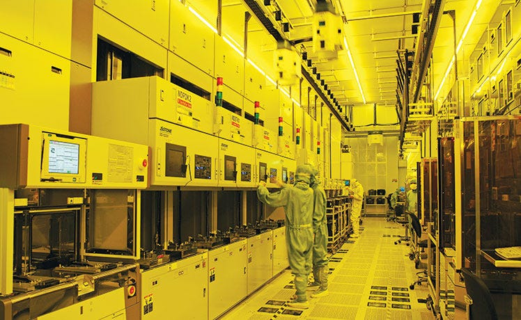
XPUs
@stocksharks_: Broadcom has emerged as a big winner in the AI boom with its XPU accelerator chips—cheaper and simpler than Nvidia’s GPUs, but built to run specific AI programs with high efficiency
We expect the stock to trade up following a solid quarter with guidance above the Street, despite elevated expectations heading into the quarter.
We believe the most significant development was Broadcom's announcement that it has converted another new custom silicon customer focused on inference, which is expected to help drive "material" upside to management's prior expectation of Al Semiconductor revenue growth of -60% in 2026. The company's Al Networking prospects remain compelling heading into 2026 with significant scale-up and scale-out opportunities driven by its Tomahawk 6 and Jericho 4 products.
Management noted that it currently has a total backlog of over $110bn, which implies significant business visibility over the next two years. Finally, the company announced that CEO Hock Tan has announced his intention to remain CEO through at least 2030. We remain Buy rated on Broadcom as we see the company remaining the leader in Al custom compute and merchant networking silicon (which is likely to grow in importance), and we believe the company's enterprise software portfolio is under appreciated
ft.com (9/4/25): OpenAI committing to $10bn in orders of the new “XPUs”, to be used internally.
@PatrickMoorhead (3/21/24): Here’s another fun one. The guy who’s smiling (Frank Ostojic) runs @Broadcom’s custom silicon group. He should be smiling as he announced that he has a third XPU design from a large “consumer AI company.” To the right is a close up of the XPU. You can see the 2 compute units on the center and all the HBM to the left and right. A full up custom SoC with lots and lots of compute, HBM, very high speed intra chip connectivity and, as you’d expect, the highest performance external networking.
@PatrickMoorhead (3/21/24): Some fun pics from the @Broadcom AI investor day today. This is obviously a wafer in its protective case. This “XPU” (AI accelerator) chip uses a 3D package. The top die is a 700mm2 accelerator on top of an 800m2 SRAM. Yes I’m surprised as: A/ I don’t know $AVGO had 3D chops. (It does). B/ I didn’t know the company did SOCs (I mistakenly thought its XPUs were ASICs like networking) Its XPUs are full SoCs with an accelerator, HBM, BOATLOADS of networking and PHYs
🙂
☑️ #95 Sep 2, 2025
VEU reversal
siliconangle.com: [Excerpt] US limits TSMC’s ability to send chipmaking equipment to its fabs in China.
The Taiwanese company uses hardware from several U.S. equipment suppliers to power its fabs. One of the largest companies on the list, Applied Materials Inc., makes machines for the deposition and etching phases of the chip production workflow. The company’s systems can deposit various materials on a silicon wafer and then form them into transistors.
TSMC also counts Milpitas, California-based KLA Corp. as a supplier. The latter company makes equipment for monitoring the reliability of chip production lines. Shares of KLA and Applied Materials dropped 3% and 2%, respectively, today on the revocation of TSMC’s VEU authorization.
“While we are evaluating the situation and taking appropriate measures, including communicating with the US government, we remain fully committed to ensuring the uninterrupted operation of TSMC Nanjing,” TSMC said in a statement today.
The Commerce Department previously revoked the VEU licenses of SK hynix Inc. and Samsung Electronics Co., the world’s two largest memory suppliers. Officials stated at the time that the companies may continue operating their fabs in China, but won’t be permitted to make upgrades or add manufacturing capacity. SK hynix maintains a flash chip facility in Nanjing that it bought from Intel Corp. a few years ago.
bis.gov > Federal Register Notices (update; 9/2/25): [Excerpt] [FR Citation: FR 42321] Revocation of Validated End-User Authorizations in the People's Republic of China.
In this final rule, the Bureau of Industry and Security (BIS) amends the Export Administration Regulations (EAR) to revise the existing Validated End-User (VEU) Authorizations list for the People's Republic of China (PRC) by removing Intel Semiconductor (Dalian) Ltd; Samsung China Semiconductor Co. Ltd; and SK hynix Semiconductor (China) Ltd.
media.bis.gov (8/28/25): [Excerpt] Department of Commerce Closes Export Controls Loophole for Foreign-Owned Semiconductor Fabs in China.
WASHINGTON, D.C. — Today, the Department of Commerce’s Bureau of Industry and Security (BIS) closed a Biden-era loophole that allowed a handful of foreign companies to export semiconductor manufacturing equipment and technology to China license-free. Now these companies will need to obtain licenses to export their technology, putting them on par with their competitors.
The loophole is known as the Validated End-User (VEU) program. In 2023, the Biden Administration expanded the VEU program to allow a select group of foreign semiconductor manufacturers to export most U.S.-origin goods, software, and technology license-free to manufacture semiconductors in China. No U.S.-owned fab has this privilege — and now, following today’s decision, no foreign-owned fab will have it either.
Former VEU participants will have 120 days following publication of the rule in the Federal Register to apply for and obtain export licenses. Going forward, BIS intends to grant export license applications to allow former VEU participants to operate their existing fabs in China. However, BIS does not intend to grant licenses to expand capacity or upgrade technology at fabs in China. Read more
koreaherald.com (8/30/25): US to require Samsung, SK hynix to acquire licenses for sending US chipmaking tools to China.
The United States Commerce Department announced a plan Friday to strip South Korean tech firms Samsung Electronics and SK hynix Inc. of "validated end-user (VEU)" status, a move that will require them to secure licenses for sending certain US chipmaking equipment to their plants in China.
On the Federal Register, the department's Bureau of Industry and Security said it will revise the existing VEU authorizations list for China by removing the companies as well as Intel Semiconductor Ltd. The department stressed its intention not to grant licenses to expand their capacity or upgrade technology at plants in China.
VEU authorization for TSMC Nanjing will be revoked effective December 31, 2025
🙂
☑️ #94 Aug 30, 2025
NEBIUS: “Yes, we are behind schedule — around two months late. Instead of 4 months, we will do it in 6. Not because of design flaws or team issues, but simply due to late deliveries from a few suppliers“
It’s been a little over a month since my last update — and here we are, about to finalize Phase 1 and soon Phase 2, with the first 50MW being delivered to our customer Nebius .
Yes, we are behind schedule — around two months late. Instead of 4 months, we will do it in 6. Not because of design flaws or team issues, but simply due to late deliveries from a few suppliers (no names here… but they know 😡).
On the other hand, some partners have been rock solid: • Carrier HVAC delivered on time and supported us every step of the way 👏 • Our internal GC team at North East Precast went above and beyond. You are LEGENDARY. Mega kudos — we love you guys! • Our engineering teams (kept discreet for a reason 😉) — you are beyond legendary. Thank you a million.
🔜 What’s next? Not much… just 300MW more to deliver in the next 6–9 months. That includes not only the Datacenter but also the Power Plant, the Cooling Plant (yes, at this scale chilled water is no longer generated inside the DC but in a dedicated mega plant)… and much more.
💡 And in about 45 days, we’ll unveil at least one innovation that will change this industry forever — and many others.
I genuinely believe you’ll love DataOne as much as we do after that (okay, I may be biased 😉). But trust me, this will blow your mind. And here’s a challenge:
👉 If anyone guesses what this innovation is, I’ll personally offer a business class ticket from wherever you live, bring you to Vineland for a full private tour, and host you for 2 days in NYC (all on me — yes, even SAF is included, we compensate carbon at DataOne).
Stay tuned. The future of datacenters is being built right here, right now. 🌍⚡
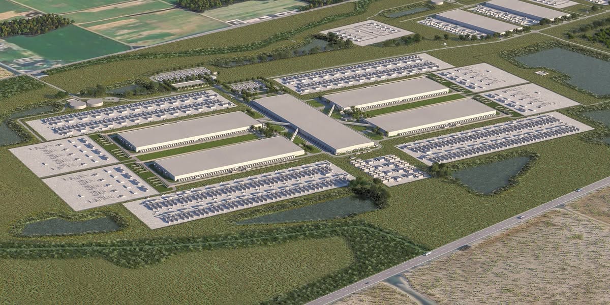
nebius.com (3/5/25): [Excerpt] We’re introducing the 300 MW New Jersey region and expanding to Iceland.
We’re thrilled to announce a major upgrade to our US-based compute capacity. To bring it to life, we’ve joined forces with DataOne, an AI hosting infrastructure company, to ensure that the first phase of the New Jersey facility goes live this summer. We’re also launching a colocation facility in Iceland with Verne, a provider of sustainably powered data centers across the Nordics, and expect it to go live this month.
New Jersey custom-built data center
The collaboration between Nebius and DataOne takes a distinctive approach to DC construction and energy efficiency. The facility will be built using Nebius’ own design, while the partnership leverages DataOne’s expertise to achieve an ambitious goal: constructing a state-of-the-art data center in just 20 weeks.
At the core of the facility is an innovative approach to power generation. We’ll leverage behind-the-meter electricity and advanced energy technology to maximize sustainability while simultaneously strengthening operational reliability — exactly what AI innovators need for their workloads.
The New Jersey site — our first major data center in the US — will go live phase by phase and is expandable up to a total of 300 MW. We previously committed to 100 MW of installed capacity by the end of 2025, and we are prepared to accelerate beyond that if required to meet demand.
• 350 MW IT load • 65 000 sqm over 44ha of land • Green Gas powered • Tier-3 compatible, ISO27001, 14001, 5001.
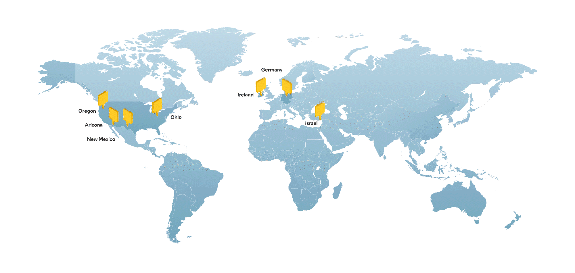
nebius.com: [Excerpt] Infrastructure for the age of AI.
Based in Amsterdam. Listed on Nasdaq. Operating worldwide.
AI is no longer a distant promise — it is becoming a defining force impacting every aspect of our lives. To fulfill its potential as a general-purpose technology that benefits all of society, AI needs purpose-built infrastructure: vast amounts of compute, optimized software and hardware, and collaborative ecosystems.
This is what Nebius builds: vertically integrated AI infrastructure that accelerates AI innovation globally and at scale. With large-scale GPU clusters deployed across Europe and the US, Nebius’s full-stack cloud platform combines the scale, flexibility and reliability of a hyperscaler with the power and performance of a supercomputer.
We serve a fast-growing ecosystem of AI innovators of all sizes — from startups to research institutes to enterprises — across sectors including healthcare and life sciences, robotics, finance and entertainment, as well as national AI programs.
The Nebius team includes hundreds of engineers with deep expertise in building world-class tech infrastructure, as well as in-house AI R&D. Headquartered in Amsterdam and listed on Nasdaq (NBIS), Nebius has a global footprint, with hubs across Europe, North America and the Middle East.
🙂
☑️ #93 Aug 30, 2025
[xAI Code Repo] xAI is already suing Li for trade secret theft, seeking damages and an injunction to stop him from using or sharing the info
@muskonomy: BREAKING: Elon Musk confirms ex-xAI engineer joined OpenAI and “uploaded xAI’s entire codebase”
The engineer had earlier sold $7M worth of his xAI stock before leaving now facing a lawsuit for stealing Grok trade secrets
“He accepted an offer at OpenAl and then uploaded our entire codebase!”
+ Related content:
@elonmusk: Not allegedly. He downloaded the entire xAI code repo, the logs prove he did it and he admitted he did it!
Misappropriating trade secrets is legally considered theft under U.S. laws like the Defend Trade Secrets Act.
🙂
☑️ #92 Aug 30, 2025 🔴 rumor
Alibaba new AI Chip: not designed for training Al models, but only for inference
wsj.com: [Excerpts] Alibaba Creates AI Chip to Help China Fill Nvidia Void. Chinese tech companies spark market exuberance by signaling they are catching up to U.S.
SINGAPORE-Chinese chip companies and artificial-intelligence developers are building up their arsenal of homegrown technology, backed by a government determined to win the Al race with the U.S.
The rapid adoption of AI across China’s economy is creating a big demand for inference—when AI programs tap their training to deliver output such as a smartphone voice assistant’s answers. Inference typically doesn’t require the most advanced chips.
Previous cloud-computing chips developed by Alibaba have mostly been designed for specific applications. The new chip, now in testing, is meant to serve a broader range of AI inference tasks, said people familiar with it.
Based on the Ascend series (Huawei Ascend) AI processor, Huawei Ascend computing includes Atlas series modules, boards, small stations, servers, clusters and other product forms, creating a full-scene AI infrastructure scheme for "end, edge, cloud". ... Based on the HUAWEI Ascend AI processor and basic software, build Atlas artificial intelligence computing solutions, including Atlas series modules, boards, small stations, servers, clusters and other rich product forms, creating a full-scene A for "end, edge, cloud" I infrastructure scheme covers the whole process of reasoning and training in the field of deep learning.
We love TPUs at Google, but GPUs are great too. This chapter takes a deep dive into the world of NVIDIA GPUs – how each chip works, how they’re networked together, and what that means for LLMs, especially compared to TPUs. This section builds on Chapter 2 and Chapter 5, so you are encouraged to read them first.
🙂
☑️ #89 Aug 25, 2025
TMSC cuts Chinese tools
@NikkeiAsia: BREAKING: TSMC will not use Chinese tools in its latest 2-nanometer chipmaking production lines -- the most advanced in the entire industry -- which will go into mass production this year.
Patrick from ServeTheHome takes us on exclusive tour of Supermicro’s cutting-edge NVIDIA B200 AI cluster, built for Lambda and housed at Cologix in Columbus, Ohio. Powered by thousands of Blackwell GPUs, 400GbE and NDR InfiniBand networking, and 10s of PB of VAST storage, our high-density CPU nodes and advanced liquid-cooling solutions deliver unparalleled performance for AI workloads. Discover how Supermicro’s innovative infrastructure is shaping the future of AI.
9:59 NVIDIA DGX GB200 NVL72 14:27 Final Words and a Hint at the Next Tour
+ Related content:
🙂
☑️ #87 Aug 20, 2025
GPUs, ASICs, and memory trends
@AlphaSenseInc: Interview with an industry expert about insights into GPUs, ASICs, and memory trends ( $NVDA, $AMD, $MU, $GOOGL ):
The expert emphasizes that GPU demand, especially for $NVDA, remains extremely strong and unchanged in terms of availability or lead times. He stresses that $AMD is also ramping quickly, with the MI300 and 400 series GPUs growing at around 15–20% year-over-year; however, adoption is concentrated almost entirely among hyperscalers because $AMD's software and ecosystem are still immature.
According to the expert, $NVDA is maintaining pricing very firm, with little to no discounting, due to extremely strong demand, while deep learning ASIC start-ups are offering discounts in the 10–20% range, primarily targeting non-hyperscaler and international customers seeking to build domestic AI infrastructure. He stresses that this discounting is less about performance and more about positioning on price, as these smaller players try to carve out market share outside the core hyperscaler segment.
In relation to ASICs, expert explained that hyperscalers build their own ASICs, such as $GOOGL's TPU, almost exclusively for internal use, while start-ups target the merchant market. However, because hyperscalers rely on in-house chips or established GPU providers like $NVDA and $AMD, the addressable market for these start-ups is shrinking. He stresses that this makes opportunities increasingly narrow, especially as $NVDA and $AMD combine hardware strength with massive investments in software and ecosystem support.
The expert emphasizes that HBM remains one of the most significant bottlenecks in the AI semiconductor supply chain, with only three major vendors; SK hynix, Samsung, and Micron producing HBM3 and HBM3E. He notes that supply from all three sources is fully allocated through 2025, and lead times for new demand are now approaching 12 months. These suppliers prioritize $NVDA first, then the hyperscalers, which leaves start-up ASIC vendors struggling to secure capacity.
He explains that HBM3 pricing has already increased by 20–30% year-over-year, driven by both extreme demand and the fact that each new GPU or ASIC generation requires significantly more HBM content. Looking forward, he expects continued upward pressure on pricing as vendors invest heavily in advancing to HBM4, which will double I/O bandwidth and density.
The expert stresses that while the overall AI semiconductor market is expanding rapidly, $AMD has been the clear share gainer, now reaching an estimated 5%–10% share and around $7–8 billion in GPU revenue. He emphasizes that this hasn’t reduced $NVDA's revenue but has modestly slowed its growth as $AMD ramps new products.
META: Our data centers with AI-optimized design, the first of which is slated to come online in 2026
about.fb.com: [Excerpt] Meta’s Kansas City Data Center and Upcoming AI-Optimized Data Centers
Developing the Next Generation of Our Data Centers
The grand opening of this data center represents a pivotal moment as we invest in scalable infrastructure optimized for our global work in AI. Our data centers with AI-optimized design, the first of which is slated to come online in 2026, will blend high-performance and flexibility with a mix of custom hardware solutions. These data centers also leverage AI solutions to prioritize resource efficiency as we develop new technologies and expand our work building the future of human connection.
We are excited to announce the Meta Kansas City Data Center is now serving traffic. That means this data center is now part of our global infrastructure that brings our technologies and programs to life, making it possible to connect billions of people worldwide.
Since breaking ground in 2022, we’ve been proud to call Kansas City, Missouri home. We chose Kansas City because it offered excellent infrastructure, a robust electrical grid, a strong pool of talent for construction and operations jobs, and incredible community partners. Construction of the Kansas City Data Center has resulted in an average of 1,500 skilled trade workers on site at peak, and the data center will support more than 100 operational jobs once completed. This facility represents an investment of more than $1 billion in the state of Missouri.
From the beginning, we have been committed to being an active partner in the Kansas City community to support its long-term vitality. Since we broke ground in 2022, we have enjoyed a strong partnership with this community, providing more than $1 million in direct funding to Clay County, Platte County and City of Kansas City Missouri schools and nonprofits, including through our annual Data Center Community Action Grants.
Meta approaches data center sustainability from the ground up — from design and construction to operations. We prioritize water stewardship with our Kansas City Data Center using a cooling technology that is significantly more water efficient than the industry standard. Plus, the data center captures and infiltrates rainwater on site and incorporates water-saving fixtures and technologies within data center facilities.
Like at all of our data centers, the Kansas City Data Center’s electricity use is matched with 100% clean and renewable energy. And, we’re proud to say that our data center buildings are LEED Gold certified — achieving very high standards for energy efficiency, water conservation, supply chain responsibility and recycling.
Here's what people are saying about today's opening event:
“Meta’s investment in Kansas City is a clear signal that our city is a place where innovation, talent, and community come together. We look forward to working with Meta to ensure this development integrates well with our community priorities and delivers meaningful benefits for Kansas City residents." - Mayor Quinton Lucas
“Meta’s grand opening in Kansas City is a powerful testament to Missouri’s ability to attract and support the most innovative companies in the world. This investment brings transformative technology, high-quality jobs, and lasting economic impact to our state, and we are proud that Meta chose Missouri as a key part of its future.” - Subash Alias, CEO, Missouri Partnership
🙂
☑️ #85 Aug 14, 2025
Intel loses key engineers to Samsung amid restructuring and project cancellations
biz.chosun.com: [Excerpt] Engineers flock to competitors as Intel's financial woes deepen and projects are shelved.
Industry observers predict that Intel will continue to see personnel losses as it cancels or reduces previously announced foundry-related investments and plans for new factories. CEO Pat Gelsinger previously noted, “Unfortunately, the investment in production capacity that Intel made over the past few years has been an excessive investment that vastly exceeds demand, and it cannot be considered prudent,” indicating that the direction of next-generation technology development will be adjusted.
However, advice has also emerged from within and outside Samsung to focus on 'filtering out the best' according to the division’s manpower demands. A senior official at Samsung commented, “Instead of blindly scouting based solely on the Intel brand, a careful process to select individuals suited to the needed processes is essential,” adding that “since Intel has a rich talent pool with extensive research in all semiconductor processes, we should seek ways for large-scale workforce reductions to benefit Samsung.”
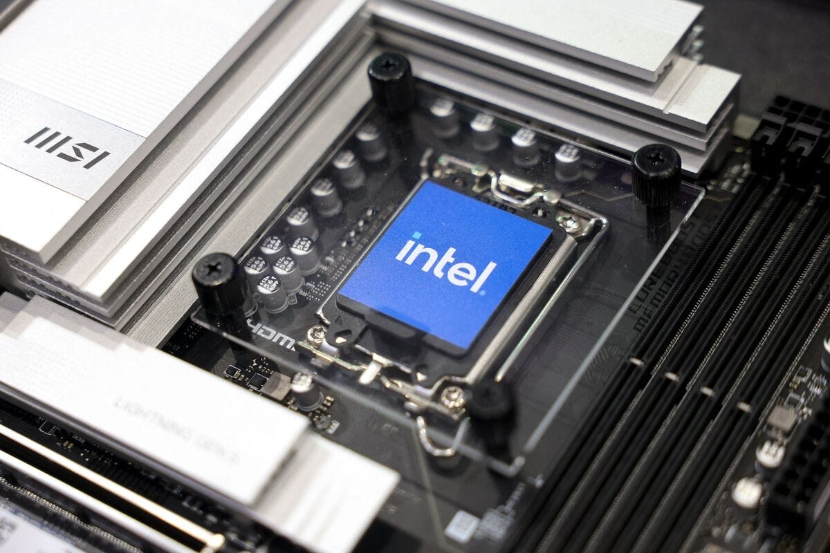
newsroom.intel.com (update; 8/22/25): Intel and Trump Administration Reach Historic Agreement to Accelerate American Technology and Manufacturing Leadership.
The government’s equity stake will be funded by the remaining $5.7 billion in grants previously awarded, but not yet paid, to Intel under the U.S. CHIPS and Science Act and $3.2 billion awarded to the company as part of the Secure Enclave program. Intel will continue to deliver on its Secure Enclave obligations and reaffirmed its commitment to delivering trusted and secure semiconductors to the U.S. Department of Defense. The $8.9 billion investment is in addition to the $2.2 billion in CHIPS grants Intel has received to date, making for a total investment of $11.1 billion
8.01 - Other Events (The registrant can use this Item to report events that are not specifically called for by Form 8-K, that the registrant considers to be of importance to security holders.)
9.01 - Financial Statements and Exhibits
🙂
☑️ #84 Aug 14, 2025
Difficulties of training the start-up’s latest system with Huawei’s semiconductors highlight dependence on Nvidia
@JamesEagle17: I had to triple-check this. It's common knowledge that DeepSeek and Chinese AI is catching up with the US. But 5 years of supercomputer data show that the opposite is actually happening. In fact, the US is smashing it out the par.
Data center energy consumption has reached a record 5% of total US power demand.
This increase has been driven by the rapid adoption of digitalization and AI technologies.
This percentage is now estimated to more than DOUBLE over the next 5 years, according to McKinsey.
Additionally, data center load is set to account for up to 40% of net new demand added until 2030.
Overall, electricity demand for data centers is expected to grow at a compounded annual growth rate of +23% through 2030.
Energy will soon be the AI bottleneck
🙂
☑️ #82 Aug 11, 2025
Lip-Bu Tan moment: Walden’s Chinese Chip Empire
Intel CEO said to visit visited White House this Monday
Reporting live from Washington, DC (just dropped my son off for law school) and got this money shot of the Intel CEO (and @cnbc) walking in to the Whitehouse! $INTC
@economicsnoah (8/7/25): In March, @eliotcxchen and I were the first to extensively report the scale of Intel CEO Lip-Bu Tan's investments in China. We tracked at least 77 portfolio companies of Tan's VC Walden International. Today President Trump called for Tan's resignation, calling him "CONFLICTED.
@SenTomCotton (8/6/25): The new CEO of @intel reportedly has deep ties to the Chinese Communists. U.S. companies who receive government grants should be responsible stewards of taxpayer dollars and adhere to strict security regulations. The board of @Intel owes Congress an explanation.
🙂
☑️ #81 Aug 8, 2025
Lip-Bu Tan moment
@SemiAnalysis_: Intel Board Issues In light of the recent journal post about the board we cannot emphasis this enough - Yeary is not fit for the job in the slightest. We wrote about how the Intel board systematically destroyed America's first great semiconductor company over a decade of mismanagement. Yeary was there the entire time.
It is Yeary not LBT who needs to leave Intel. Reminder for everyone, Yeary wants to spin the foundry, while he has no semiconductor experience and was on the board for the entire 10nm debacle. read more:
newsroom.intel.com (8/7/25): [Excerpt] My commitment to you and our company. The following note from Lip-Bu Tan was sent to all Intel Corporation employees on August 7, 2025:
Dear Team,
I know there has been a lot in the news today, and I want to take a moment to address it directly with you.
Let me start by saying this: The United States has been my home for more than 40 years. I love this country and am profoundly grateful for the opportunities it has given me. I also love this company. Leading Intel at this critical moment is not just a job – it’s a privilege. This industry has given me so much, our company has played such a pivotal role, and it's the honor of my career to work with you all to restore Intel's strength and create the innovations of the future. Intel's success is essential to U.S. technology and manufacturing leadership, national security, and economic strength. This is what fuels our business around the world. It’s what motivated me to join this team, and it’s what drives me every day to advance the important work we’re doing together to build a stronger future.
There has been a lot of misinformation circulating about my past roles at Walden International and Cadence Design Systems. I want to be absolutely clear: Over 40+ years in the industry, I’ve built relationships around the world and across our diverse ecosystem – and I have always operated within the highest legal and ethical standards. My reputation has been built on trust – on doing what I say I’ll do, and doing it the right way. This is the same way I am leading Intel.
newsroom.intel.com (8/7/25): [Excerpt] Our commitment to advancing U.S. national and economic security.
Intel, the Board of Directors, and Lip-Bu Tan are deeply committed to advancing U.S. national and economic security interests and are making significant investments aligned with the President's America First agenda. Intel has been manufacturing in America for 56 years. We are continuing to invest billions of dollars in domestic semiconductor R&D and manufacturing, including our new fab in Arizona that will run the most advanced manufacturing process technology in the country, and are the only company investing in leading logic process node development in the U.S. We look forward to our continued engagement with the Administration.
We will focus our AI efforts on developing a cohesive silicon, system and software stack strategy. In the past, we have approached AI with a traditional, silicon- and training-centric mindset. This needs to change – and we have already started incubating new capabilities while attracting new talent.
As we make this shift, we will concentrate our efforts on areas we can disrupt and differentiate, like inference and agentic AI. Our starting point will be emerging AI workloads – then we will work backward to design software, systems and silicon that enable the best customer outcomes. We have a lot of work underway, and will be sharing more about our plans in the coming months.
🙂
☑️ #80 Aug 5, 2025
A possible leak of trade secrets
cnbc.com: [Excerpt] World’s largest chipmaker TSMC says it has discovered potential trade secret leaks.
Taiwan Semiconductor Manufacturing Co. said it had detected “unauthorized activities” that led to the discovery of potential trade secret leaks.
TSMC said it has taken action against the personnel involved and launched legal proceedings.
The world’s biggest semiconductor manufacturer dominates the market for the manufacturing of the most advanced chips and counts major firms like Apple and Nvidia as clients.
TSMC workers walk down a hallway in a chipmaking fab in Taiwan. The company is building three such plants in Arizona. Source: TSMC via CNBC LLC
asia.nikkei.com: TSMC fires workers for breaching data rules on cutting-edge chip tech.
TAIPEI -- Taiwan Semiconductor Manufacturing Co. has fired several employees for violating rules on obtaining sensitive information related to cutting-edge chip technology and initiated legal action over the matter, Nikkei Asia learned
esg.tsmc.com (7/14/22): TSMC Establishes the "Trade Secret Registration System Alumni Association" to Comprehensively Upgrade Industrial Competitiveness.
Source: Taiwan Semiconductor Manufacturing Company Limited
28-nanometer fabrication process (2018)

It is not the first time that TSMC has been the target for potential theft. In 2018, a Taiwanese court indicted a former employee for copying trade secretes related to the 28-nanometer fabrication process, with intent to transfer them to a semiconductor company in mainland China.
🙂
☑️ #79 Jul 30, 2025
META: If the true economic life on its GPU’s is actually 2-3 years, most of its “profits” are materially overstated
@RealJimChanos: It looks like $META’s depreciable life on its capital base ($210B at 6/30/25) was 11-12 years, as of the 2Q. If the true economic life on its GPU’s is actually 2-3 years, most of its “profits” are materially overstated.
(2) Put another way, $META increased its capital base 45% Y/Y in the 2Q, from $145B to $210B, or $65B. Yet annualized D&A increased only $2.8B ($700M x 4) in the recent 2Q. That’s 22-year life, on the margin. Whatever you think of the stock price here-that’s patently absurd.
(3) I would also note that $META is now growing its capital base more than 2x its revenues, 45% vs 21%. And for those of you posting/asking, we have NO short position/recommendation in $META.
Oklo and Liberty Energy partnering to combine nuclear, gas, and grid services into a single solution for data centers and industrial customers
@oklo: Oklo and Liberty Energy partnering to combine nuclear, gas, and grid services into a single solution for data centers and industrial customers.
A next-generation energy model backed by deep operational experience and built for scale.
+ Related content:
oklo.com: [Excerpt] Oklo and Liberty Energy Launch Next-Generation Integrated Power Solution.
Liberty’s Forte natural gas power generation and load management solution will provide initial reliable primary power and flexible energy services, along with future grid management services focused on optimization and resiliency. As Oklo’s Aurora powerhouses come online, they will be integrated to provide clean, continuous baseload energy, complementing Liberty’s natural gas power.
🙂
☑️ #77 Jul 14, 2025
Prometheus & Hyperion Data Centers
facebook.com > Mark Zuckerberg: For our superintelligence effort, I'm focused on building the most elite and talent-dense team in the industry. We're also going to invest hundreds of billions of dollars into compute to build superintelligence. We have the capital from our business to do this.
SemiAnalysis just reported that Meta is on track to be the first lab to bring a 1GW+ supercluster online.
We're actually building several multi-GW clusters. We're calling the first one Prometheus and it's coming online in '26. We're also building Hyperion, which will be able to scale up to 5GW over several years. We're building multiple more titan clusters as well. Just one of these covers a significant part of the footprint of Manhattan.
Meta Superintelligence Labs will have industry-leading levels of compute and by far the greatest compute per researcher. I'm looking forward to working with the top researchers to advance the frontier!
bloomberg.com (6/30/25) via sherwood.news (7/8/25): [Excerpt] Meta poaches top Apple AI executive for its superintelligence group.
cnbc.com(6/30/25): Here is Zuckerberg’s full internal memo released Monday:
As the pace of AI progress accelerates, developing superintelligence is coming into sight. I believe this will be the beginning of a new era for humanity, and I am fully committed to doing what it takes for Meta to lead the way. Today I want to share some details about how we’re organizing our AI efforts to build towards our vision: personal superintelligence for everyone.
We’re going to call our overall organization Meta Superintelligence Labs (MSL). This includes all of our foundations, product, and FAIR teams, as well as a new lab focused on developing the next generation of our models.
Alexandr Wang has joined Meta to serve as our Chief AI Officer and lead MSL. Alex and I have worked together for several years, and I consider him to be the most impressive founder of his generation. He has a clear sense of the historic importance of superintelligence, and as co-founder and CEO he built ScaleAI into a fast-growing company involved in the development of almost all leading models across the industry.
Nat Friedman has also joined Meta to partner with Alex to lead MSL, heading our work on AI products and applied research. Nat will work with Connor to define his role going forward. He ran GitHub at Microsoft, and most recently has run one of the leading AI investment firms. Nat has served on our Meta Advisory Group for the last year, so he already has a good sense of our roadmap and what we need to do.
We also have several strong new team members joining today or who have joined in the past few weeks that I’m excited to share as well:
Trapit Bansal -- pioneered RL on chain of thought and co-creator of o-series models at OpenAI.
Shuchao Bi -- co-creator of GPT-4o voice mode and o4-mini. Previously led multimodal post-training at OpenAI.
Huiwen Chang -- co-creator of GPT-4o’s image generation, and previously invented MaskGIT and Muse text-to-image architectures at Google Research
Ji Lin -- helped build o3/o4-mini, GPT-4o, GPT-4.1, GPT-4.5, 4o-imagegen, and Operator reasoning stack.
Joel Pobar -- inference at Anthropic. Previously at Meta for 11 years on HHVM, Hack, Flow, Redex, performance tooling, and machine learning.
Jack Rae -- pre-training tech lead for Gemini and reasoning for Gemini 2.5. Led Gopher and Chinchilla early LLM efforts at DeepMind.
Hongyu Ren -- co-creator of GPT-4o, 4o-mini, o1-mini, o3-mini, o3 and o4-mini. Previously leading a group for post-training at OpenAI.
Johan Schalkwyk -- former Google Fellow, early contributor to Sesame, and technical lead for Maya.
Pei Sun -- post-training, coding, and reasoning for Gemini at Google Deepmind. Previously created the last two generations of Waymo’s perception models.
Jiahui Yu -- co-creator of o3, o4-mini, GPT-4.1 and GPT-4o. Previously led the perception team at OpenAI, and co-led multimodal at Gemini.
Shengjia Zhao -- co-creator of ChatGPT, GPT-4, all mini models, 4.1 and o3. Previously led synthetic data at OpenAI.
I’m excited about the progress we have planned for Llama 4.1 and 4.2. These models power Meta AI, which is used by more than 1 billion monthly actives across our apps and an increasing number of agents across Meta that help improve our products and technology. We’re committed to continuing to build out these models.
In parallel, we’re going to start research on our next generation of models to get to the frontier in the next year or so. I’ve spent the past few months meeting top folks across Meta, other AI labs, and promising startups to put together the founding group for this small talent-dense effort. We’re still forming this group and we’ll ask several people across the AI org to join this lab as well.
Meta is uniquely positioned to deliver superintelligence to the world. We have a strong business that supports building out significantly more compute than smaller labs. We have deeper experience building and growing products that reach billions of people. We are pioneering and leading the AI glasses and wearables category that is growing very quickly. And our company structure allows us to move with vastly greater conviction and boldness. I’m optimistic that this new influx of talent and parallel approach to model development will set us up to deliver on the promise of personal superintelligence for everyone.
We have even more great people at all levels joining this effort in the coming weeks, so stay tuned. I’m excited to dive in and get to work.
🙂
☑️ #76 Jun 27, 2025
Mitsui Fudosan to set up chip-focused development hub in Tokyo
asia.nikkei.com: [Excerpt] Initiative aims to connect companies and talent spread across Japan.
TOKYO -- Mitsui Fudosan will establish a semiconductor-focused industrial development hub in Tokyo as soon as autumn, Nikkei has learned, bringing together companies and research organizations in the sector to help foster new businesses and develop talent.
The company plans to enlist 200 to 300 organizations as members in its new group within a few years. Mitsui Fudosan aims to create a new growth field by moving beyond its role as a real estate company to become an industrial developer that can lead in bringing together industry, government and academia.
Texas Instruments plans to invest more than $60 billion to manufacture billions of foundational semiconductors in the U.S.
ti.com: [Excerpt] Leading U.S. companies Apple, Ford, Medtronic, NVIDIA and SpaceX strengthen partnerships with TI to unleash the next era of American innovation.
Backed by the strength of TI’s U.S. manufacturing presence
TI is a driving force behind the return and expansion of semiconductor manufacturing in the U.S. The company’s more than $60 billion investment in U.S. manufacturing includes building and ramping seven, large-scale, connected fabs. Combined, these fabs across three manufacturing mega-sites in Texas and Utah will manufacture hundreds of millions of U.S.-made chips daily that will ignite a bold new chapter in American innovation.
Sherman, Texas: SM1, TI’s first new fab in Sherman will begin initial production this year, just three years after breaking ground. Construction is also complete on the exterior shell of SM2, TI’s second new fab in Sherman. Incremental investment plans include two additional fabs, SM3 and SM4, to support future demand.
Richardson, Texas: TI’s second fab in Richardson, RFAB2, continues to ramp to full production and builds on the company’s legacy of introducing the world’s first 300mm analog fab, RFAB1, in 2011.
Lehi, Utah: TI is ramping LFAB1, the company’s first 300mm wafer fab in Lehi. Construction is also well underway on LFAB2, TI’s second Lehi fab that will connect to LFAB1.
Learn more
Press kit (includes images, video b-roll and fact sheet)
@TexasInstruments (6/17/25): Making progress at TI's 300mm wafer fab in Sherman, Texas.
🙂
☑️ #74 Jun 12, 2025
Micron and Trump Administration Announce Expanded U.S. Investments in Leading-Edge DRAM Manufacturing and R&D
investors.micron.com: [Excerpt] Micron Plans to Invest Approximately $200 Billion in Semiconductor Manufacturing and R&D in Idaho, New York and Virginia, Enhancing Domestic Memory Supply and Technology Leadership.
Micron to Build Second Leading-Edge Memory Manufacturing Fab in Idaho, Modernize and Expand Virginia Fab and Bring End-to-End High Bandwidth Memory (HBM) Manufacturing Capabilities to U.S. to Meet Anticipated AI-Driven Demand.
Micron’s approximately $200 billion broader U.S. expansion vision includes two leading-edge high-volume fabs in Idaho, up to four leading-edge high-volume fabs in New York, the expansion and modernization of its existing manufacturing fab in Virginia, advanced HBM packaging capabilities and R&D to drive American innovation and technology leadership. These investments are designed to allow Micron to meet expected market demand, maintain share and support Micron’s goal of producing 40% of its DRAM in the U.S. The co-location of these two Idaho fabs with Micron’s Idaho R&D operations will drive economies of scale and faster time to market for leading-edge products, including HBM.
@MicronTechnology: Micron’s approximately $200B investment plans in U.S. manufacturing and R&D | Micron Technology.
🙂
☑️ #73 Jun 11, 2025
The core team behind Lamini x AMD
@HyperTechInvest: $AMD continues the talent grab The company just announced they acquired the core team behind Lamini
Lamini helps enterprises train LLMs based on their data
They have a lot of experience deploying models with $AMD accelerators
CEO Sharon Zhou worked as a machine learning product manager at Google and will become vice president of AI at $AMD
The startup raised $25 million last year from several investors, including Andrew Ng, Dropbox CEO Drew Houston, and Lip-Bu Tan, who later became Intel’s CEO
+ Related content:
pitchbook.com: Lamini ovreview. Who are Lamini’s investors?
lamini.ai (9/26/23): [Excerpt] Lamini & AMD: Paving the Road to GPU-Rich Enterprise LLMs.
What’s more, with Lamini, you can stop worrying about the 52-week lead time for NVIDIA H100s. Using Lamini exclusively, you can build your own enterprise LLMs and ship them into production on AMD Instinct GPUs. And shhhh… Lamini has been secretly running on over one hundred AMD GPUs in production all year, even before ChatGPT launched. So, if you’ve tried Lamini, then you’ve tried AMD.
Now, we’re excited to open up LLM-ready GPUs to more folks. Our LLM Superstation is available both in the cloud and on-premise. It combines Lamini's easy-to-use enterprise LLM infrastructure with AMD Instinct™ MI210 and MI250 accelerators. It is optimized for private enterprise LLMs, built to be heavily differentiated with proprietary data.
🙂
☑️ #72 Jun 5, 2025
Oligopolies
@Invesquotes: The semiconductor industry is likely one where people tend to miss the forest for the trees
Sure, it's cyclical...but how many industries are there with so much long-term optionality where the supply chain is made up of oligopolies?
Not many is my guess!
🙂
☑️ #71 Jun 4, 2025
DRT vs Equinix
@dualedgeinvest: Coming Soon: DRT vs Equinix — A Tale of Two Data Center REITs.
One plays the long game with big acquisitions.
The other bets on steady, service-driven growth.
Different strategies. Different risks. Different rewards.
📡 Full deep-dive drops soon — subscribe now to catch it first - while it’s still free.
EQIX 0.00%↑equinix.com: [Excerpt] Equinix is the world’s digital infrastructure company.
We interconnect industry-leading organizations across a digital-first world, empowering them with trusted, secure and sustainable-minded infrastructure.
🙂
☑️ #70 Jun 2, 2025
IBM Unveils watsonx AI Labs: The Ultimate Accelerator for AI Builders, Startups and Enterprises in New York City
newsroom.ibm.com: [Excerpt] New AI initiative will co-create gen AI solutions with IBM clients, nurture NYC talent, advance enterprise AI implementations.
The lab benefits from – and helps fuel – New York City's status as a global AI hub. New York City has more than 2,000 AI startups, and its AI workforce grew by nearly 25% from 2022 to 2023, according to Tech:NYC. Since 2019, more than 1,000 AI-related companies in New York City have raised $27 billionin funding.
Also today, continuing its commitment to the local startup ecosystem, IBM announced it will acquire expertise and license technology from Seek AI, the New York City-based startup building AI agents to harness enterprise data. Seek AI helps businesses leverage agentic AI to mine value from enterprise data, and their expertise will serve as a foundational part of watsonx AI Labs.
Source: International Business Machines Corporation
seek.ai (9/26/24): [Excerpt] How to Power Your Data Strategy with Agentic AI.
There’s been a lot of buzz and excitement recently about agentic AI, the next generation of artificial intelligence systems that are set apart from traditional AI by their ability to operate autonomously and take independent action to accomplish specific goals.
First things first: with all the noise out there about agents, how do we even define them? At its most basic interpretation, IBM defined an AI agent in simple terms as, “...a system or program that is capable of autonomously performing tasks on behalf of a user or another system by designing its workflow and utilizing available tools.”
🙂
☑️ #69 Jun 2, 2025
View on U.S. “reciprocal” tariffs and the FX impact on profitability?
pr.tsmc.com > TSMC Shareholders’ Meeting Resolutions > @x.com/rwang07: Memo note on TSMC Shareholders Meeting (Q&A) Hosted by CEO C.C. Wei on June 3, 2025.
The company has pledged to run on 100 % renewable energy by 2040. Has it invested in renewable‑energy projects?
Green power is in short supply in Taiwan. TSMC has considered building its own facilities but must follow legal requirements. For now, it invests in green power wherever possible. TSMC currently pays one of the country’s highest electricity rates and also helps its supply chain adopt green power. Taiwan will start collecting a carbon fee next year. We fully support renewable energy and will buy all the green power we can obtain.
Will Taiwan’s recent electricity‑price hikes delay the use of green power?
Costs will indeed rise, but TSMC is highly profitable and can absorb them. TSMC’s overseas fabs already usage rate of green power is reaching 100%, while usage in Taiwan lags badly. Whenever green power is available, we will definitely use it; if necessary, we will give the green‑energy sector long‑term commitments. We will disclose any sustainability information to investors and stakeholders. By 2030 we will disclose our annual renewable‑energy usage each year.
View on U.S. “reciprocal” tariffs and the FX impact on profitability?
Every 1 % appreciation of the NT dollar trims our gross margin by 0.4 %. An 8 % rise has reduced margin by a little over 3 %. We can only keep working hard and charge the value we deserve. Tariffs affect us somewhat but indirectly; lower demand hurts business, though AI demand is still greater than supply. We fear nothing except a global economic slump. We are maintaining 25 % growth, and earnings will hit a record high this year.
Will technology be stolen if we build fabs overseas?
No. Our know‑how comes from 10 000 R&D engineers and 10 000 production‑improvement staff. New technology is first installed in a “mother fab,” refined for six to twelve months, then moved into volume production. If we are confident about building fabs worldwide, we are confident the technology will not leak.
The return on TWSE:2330 trails NYSE:TSM by a wide margin?
The two prices always differ, but the trends are the same. Share prices are driven by supply and demand. In the near term we are not considering conversion between ADRs and common shares.
How are humanoid‑robot chip orders?
They have already started and are strong. We are also using AI to enhance our own capabilities—business is doing very well.
Could capacity become excessive?
Our customers are very aggressive. We have an excellent planning system to gauge real demand and have recently begun talking with our customers’ customers. US $40 billion in capex is huge—we act very carefully to avoid mistakes.
How do U.S. production lines replicate Taiwan fabs?
The Yields are identical; costs differ.
Capital expenditure and cash flow
Our dividend policy is stable and growing. We pay out 70 % of free cash flow as cash dividends. Once investments start paying back, dividends will rise faster.
Building a supercomputer with NVIDIA and Foxconn?
We are working closely with both companies.
Rapid AGI development and TSMC?
AI consists of software and hardware; software progress needs hardware support. All AI customers worldwide must cooperate with TSMC. We take responsibility for providing enough chips and are striving to meet their demand.
On Huawei's Chips
Frankly, we cannot claim complete control. We do our best to comply with laws and regulations and check whether the products we manufacture (for customers) violate any rules.
U.S. requests for technology transfer?
Our technology will not be stolen.
On Middle East and Rumor of Setting up Fab
We will not build fabs there. Competitors in that region are also our customers, and we will treat them well.
Depreciation (equipment) policy
TSMC's equipment is fully depreciated within five years. Depreciation is a non‑cash item and does not affect ROE. Dividends are based on free cash flow.
Impact of supplier Asahi Kasei in Japan and full support for TSMC?
We will certainly help wherever we can in Taiwan.
Earthquake‑risk assessment
TSMC production lines are the world’s most robust. We have internal risk management and close cooperation with local governments. No need to worry—TSMC always recovers the fastest after natural disasters.
Will TSMC raise prices significantly to cover tariffs and overseas‑fab costs?
What we think internally we cannot say aloud.
Traffic issues at the Kumamoto fab?
We keep working with the government to improve transportation; each site location has been fully discussed with local residents and authorities.
TSMC’s outlook for the next 5–10 years?
Extremely positive.
🙂
☑️ #68 May 31, 2025
SAIMEMORY: SoftBank, Intel work on AI memory chips that use half as much power
asia.nikkei.com: [Excerpt] TOKYO -- SoftBank and Intel are developing a type of memory for artificial intelligence expected to consume much less electricity than current chips, helping to build efficient AI infrastructure in Japan.
The companies plan to develop a structure for stacked DRAM chips that uses a different wiring structure than current advanced high-bandwidth memory, slashing power consumption by roughly half.
newsonjapan.com: [Excerpt] SoftBank Startup Aims to Revolutionize AI Chips.
The Japanese government, which has enacted legislation allocating more than 10 trillion yen to support next-generation semiconductor and AI development, is expected to back SAIMEMORY’s production efforts as part of this broader policy push. This suggests that SAIMEMORY, like Rapidus before it, could become a future recipient of state support.
In an interview with TV Tokyo, SoftBank’s head of semiconductor development expressed confidence in the project, citing strong demand for low-power, low-cost memory solutions. When asked about potential collaboration with Rapidus, the spokesperson said it would depend on future technical developments but expressed optimism that the partnership could work.
University of Tokyo are also participating in the project.
🙂
☑️ #67 May 27, 2025
New consortium wants to build AI Gigafactory
@handelsblatt.com: [Translated] [Excerpt] They are the factories of the future: the EU is supporting the construction of data centers for artificial intelligence. German corporations are negotiating a consortium for such an AI Gigafactory.
According to Handelsblatt information, SAP, Deutsche Telekom, Ionos, the Schwarz Group and Siemens are negotiating a joint application to the European Union (EU) for such a gigantic data center for AI applications. There are intensive discussions, five managers from the industry reported.
At the conference "Technology Experience Convention Heilbronn" (TECH), an initiative founded by the Handelsblatt Media Group in cooperation with Schwarz Digits, SAP board member Thomas Saueressig said about the AI project:
"It is only possible in partnership, that is quite clear. Which model is the right one is currently being discussed."
Ionos CEO Achim Weiß said the initiative was an "important step for more digital sovereignty". Therefore, they will participate in a corresponding tender. And Rolf Schumann, Chief Digital Officer of the Schwarz Group, emphasized in a panel discussion: "We hope that we will bring everyone together, manage the matter and get it through together."
g42.ai : [Excerpt] G42 to lead a consortium with US partners to build 5GW UAE-US AI Campus.
Built by G42 in partnership with U.S. technology leaders, the UAE-US AI Campus will deliver sovereign, AI-grade compute at scale, supporting regional innovation and serving nearly half the world’s population.
wam.ae: [Excerpt] UAE, US Presidents attend unveiling of Phase 1 of new 5GW AI campus in Abu Dhabi.
The UAE-US AI campus will include 5GW of capacity for AI data centres in Abu Dhabi, providing a regional platform from which US hyperscalers will be able to offer latency-friendly services to nearly half of the global population.
Once completed, the facility will leverage nuclear, solar, and gas power to minimise carbon emissions and will also house a science park driving advancements in AI innovation.
The campus will be built by G42 and operated in partnership with several US companies. The endeavour builds on a new framework by the two countries’ governments – the US-UAE AI Acceleration Partnership – to deepen cooperation and collaboration on AI and advanced technologies.
cnbc.com (update; 5/16/25): Nvidia, Cisco, Oracle and OpenAI are backing the UAE Stargate data center project.
U.S. tech giants Nvidia, Cisco, Oracle and OpenAI are supporting the “UAE Stargate” artificial intelligence data center announced this week, multiple people familiar with the deal confirmed Friday
The new AI campus, the largest outside the US, will be home to US hyperscalers and large enterprises that can leverage the capacity for regional ‘compute resources’ with the ability to serve the Global South.
🙂
☑️ #65 May 13, 2025
Japan: The 2-Nanometer Challenge
japan-forward.com: [Excerpt]: Rapidus Begins 2-nm Chip Pilot Production, Vital for Japan's Tech Future.
Mass Production Challenges
The first prototypes are expected between mid- and late-July. Rapidus will begin by producing standard chips using IBM's technology. Customer-specific prototypes will follow, with the goal of delivering them within fiscal 2025.
To improve yield — the ratio of usable chips — Rapidus is using a method called "batch-type" or "single-wafer processing," in which wafers are handled one at a time. While not ideal for mass production, this approach allows real-time feedback to the design team. Defects can be quickly addressed, enabling faster improvement of the yield rate.
In a push to promote the domestic production of microchips, the Japanese government has funded the Rapidus project with over ¥900 billion JPY ($5.75 billion USD) so far. Private companies like Toyota and Sony have also invested in the startup. The aim is for Japan to compete with global leaders like Taiwan and South Korea.
Koike is confident that Rapidus can pull this off. "The 2-nm technology will change our lives," he adds. He points to Hokkaido's agricultural sectors where farms are struggling to find workers and farmers are getting old with little hope of finding young people who want to take over their business. Koike hopes that the AI chip will help overcome problems faced by aging societies. With AI, fully automated farms could raise livestock or grow food in the future.
Fundamental to this is the tiny AI chips that Rapidus wants to mass produce. Only the 2-nm chip can provide the speed needed to process the huge amount of data needed to run complex operations like a robotic farm or self-driving cars and trucks.
Update (5/19/25): More than half of Japan's seven new semiconductor plants (facilities completed since fiscal year 2023) remain inactive, Nikkei reported citing industry data.
🙂
☑️ #64 May 12, 2025
147 zettabytes annually
@probnstat: As of 2025, the world generates approximately 402.74 million terabytes of data every single day. This staggering amount equates to about 147 zettabytes annually, underscoring the immense scale at which information is being created, captured, and consumed globally.
To put this into perspective, this daily data generation is equivalent to streaming over 100 million high-definition movies simultaneously. The surge is largely driven by the proliferation of digital platforms, the Internet of Things (IoT), and the increasing digitization of services across sectors.
This exponential growth in data not only reflects our increasing reliance on digital technologies but also presents challenges and opportunities in data management, storage, and analysis.
Data Centers drive record surge in tech investment
@bespokeinvest: Data center investment added a full percentage point to GDP in Q1; a record.
🙂
☑️ #62 Apr 29, 2025
Direct Connect 2025 Keynote
@Intel: Direct Connect 2025 will bring together executive leaders, customers, industry technologists, and ecosystem partners for an exclusive event focused on the future of technology and innovation on April 29th, 2025. Join us via livestream for the morning keynotes, starting with an opening address from our CEO, Lip-Bu Tan. This will be followed by a joint presentation from Naga Chandrasekaran, EVP, CTO, GM, and Ann Kelleher, EVP, Foundry Technology & Manufacturing. Kevin O’Buckley, SVP, GM, Foundry Services, will conclude the morning sessions with a summary of our progress over the past year. Direct Connect 2025 promises to be a pivotal gathering, showcasing how our solutions address complex challenges, drive innovation, and optimize operational efficiency. Don't miss this opportunity to gain valuable insights and be part of the conversation shaping the future.
🙂
☑️ #61 Apr 28, 2025
Huawei hopes the newest in the series of its Ascend Al processors, Ascend 910D, will be more powerful than Nvidia's H100
wsj.com: [Excerpt] China’s Huawei Develops New AI Chip, Seeking to Match Nvidia. Superpower rivalry over semiconductors heats up despite Washington’s attempts to block Beijing.
This year, Huawei is poised to ship more than 800,000 Ascend 910B and 910C chips to customers including state-owned telecommunications carriers and private AI developers such as TikTok parent ByteDance, people familiar with the matter said. Some buyers have already been in talks with Huawei to increase orders of the 910C after the Trump administration restricted the exports of Nvidia’s H20s, the people said.
Despite manufacturing bottlenecks, Huawei and several Chinese chip firms have already been able to deliver some products comparable to Nvidia chips, albeit with a lag of a few years. Chip makers have been turning to technologies that can pack several chips together to create more powerful processors, as it gets harder and more expensive to make the circuitry inside chips smaller.
Huawei hopes the newest in the series of its Ascend Al processors, Ascend 910D, will be more powerful than Nvidia's H100.
🙂
☑️ #60 Apr 24, 2025
How to power the explosive growth of artificial intelligence with reliable, scalable American energy
news.okstate.edu: [Excerpt] National leaders convene to address energy imperative behind America’s AI revolution.
In a landmark event, leaders from technology, energy and academia convened Thursday at Oklahoma State University’s Hamm Institute for American Energy for the Powering AI: Global Leadership Summit.
The one-day, high-level summit focused on solving one of the most pressing challenges of our time: how to power the explosive growth of artificial intelligence with reliable, scalable American energy.
Hosted by the Hamm Institute, the summit marks the first time these three critical industries have united to build a collaborative strategy for the AI age. In a rapidly evolving technological landscape, attendees focused on the infrastructure, power systems and policy innovation needed to support the U.S. as a global leader in artificial intelligence and big data.
“AI is pushing the boundaries of what’s possible—but without the infrastructure to scale it, we’re only scratching the surface,”
By building capacity now, we position the United States to lead in an era where computational intelligence becomes a defining element of national strength and societal wellbeing.”
Anthropic co-founder Jack Clark
"There's been no significant change" in the market. Kevin Miller, Amazon's Vice President of Global Data Centers
The company is experiencing "tremendous growth" in this sector. Josh Parker, Nvidia's Senior Director of Corporate Sustainability
TSMC reports major losses in Arizona following strong performance in China
@BarrettYouTube: TSMC has racked up over US 1.2 billion in losses at its Arizona fabs over the past four years, even as its Nanjing plant in China turned a profit last year. Meanwhile, the company also lost billions in Japan and Europe.
Despite the mounting losses, TSMC just pledged another $100B investment in the U.S., in what’s being called the largest single foreign investment in American history. Trump even admitted he threatened 100% tariffs if TSMC didn’t build in the U.S.
Critics in Taiwan are calling it a repeat of how the U.S. crushed Japan’s chip industry in the ’80s, accusing local leaders of blindly handing over Taiwan’s tech advantage without negotiating returns.
Beijing weighed in too, with the Taiwan Affairs Office saying the DPP is using TSMC as a tool in its “rely on America for independence” play—and calling out Taiwan’s leadership for “selling out” the island’s semiconductor crown jewel.
+ Related content:
dimsumdaily.hk [Excerpt] According to the company’s latest annual shareholder report, TSMC’s plant in Arizona incurred a loss of 14.3 billion New Taiwan dollars (approximately 440 million US dollars) last year, marking the highest annual loss since the company began its investments in US manufacturing. Over the past four years, TSMC has accumulated losses exceeding 39.4 billion New Taiwan dollars at this site.
The company’s other overseas ventures also faced difficulties. Its advanced chip manufacturing facility in Japan recorded a loss of 4.38 billion New Taiwan dollars in 2024, while a joint venture in Germany reported a loss of 556 million New Taiwan dollars.
In stark contrast, TSMC’s operations on the Chinese mainland have performed well, with the Nanjing plant alone generating a profit of 25.95 billion New Taiwan dollars in 2024. Altogether, profits from mainland operations have surpassed 80 billion New Taiwan dollars over the past four years.
TSMC Unveils Next-Generation A14 Process at North America Technology Symposium. Showcasing TSMC’s latest offerings for high performance computing, smartphone, automotive, and IoT applications Taiwan Semiconductor Manufacturing.
Company Limited (TSMC) unveiled on Wednesday its "next cutting-edge logic process technology, A14," at the North America Technology Symposium.
"Representing a significant advancement from TSMC's industry-leading N2 process, A14 is designed to drive Al transformation forward by delivering faster computing and greater power efficiency. It is also expected to enhance smartphones by improving their on-board Al capabilities, making them even smarter," TSMC detailed.
🙂
☑️ #57 Apr 17, 2025
World’s fastest memory writes 25 billion bits per sec, 10,000× faster than current tech
Researchers from Shanghai-based Fudan University have developed a picosecond-level flash memory device with an unprecedented program speed of 400 picoseconds, equivalent to operating 25 billion times per second, shattering the existing speed limits in information storage.
It became the fastest semiconductor charge storage device currently known to humanity, and scientists said such a breakthrough will have important application values to assist the ultra-fast operation of large artificial intelligence models.
interestingengineering.com: [Excerpts] PoX could be the key to unlocking performance bottlenecks caused by storage limitations in AI hardware.
Industrial and strategic implications.
Flash memory remains a cornerstone of global semiconductor strategy thanks to its cost and scalability. Fudan’s advance, reviewers say, offers a “completely original mechanism” that may disrupt that landscape.
If mass‑produced, PoX‑style memory could eliminate separate high‑speed SRAM caches in AI chips, slashing area and energy. It can enable instant‑on, low‑power laptops and phones, and support database engines that hold entire working sets in persistent RAM.
🙂
☑️ #56 Apr 10, 2025
Crusoe Cloud AI origins
forbes.com: [Excerpt] Meet The Tiny Startup Building Stargate, OpenAI’s $500 Billion Data Center Moonshot. Crusoe Energy got its start harnessing oilfield flare gas to mine bitcoin. So how did cofounders Chase Lochmiller and Cully Cavness end up building the first phase of the world’s biggest AI datacenter – $500 billion Project Stargate – for OpenAI and Oracle?
That set up Crusoe for its leap to AI. In 2023, Crusoe borrowed $200 million to purchase coveted Nvidia H100 GPUs to expand its nascent cloud computing services and hired talent from the likes of datacenter giants 365 Main and Digital Realty. They topped off the year by partnering with Iceland’s AtNorth data center developer to set up their Crusoe Cloud services in the frigid country (making it easier to cool off GPUs). "Crusoe is building datacenters larger than Digital Realty ever did," marvels former CEO Bill Stein, now a Crusoe board member. Key to their longterm success, he says, will be "signing 15 year leases where counterparty risk is minimal," like with Stargate.
Crusoe’s shot at the big time came in the first quarter of 2024. Lochmiller had learned that some tech giants, believed to be OpenAI and Microsoft (he declines to say who) were shopping for contractors to build an AI-specialized, hyperscale datacenter, and do it fast. Other developers balked at the ludicrous timetable of less than two years. Land acquisition, permits, supply chain lead times, all looked impossible.
crusoe.ai (3/18/25): [Excerpt] Crusoe Expands AI Data Center Campus In Abilene To 1.2 Gigawatts.
SAN FRANCISCO, CA / ABILENE, TX / March 18, 2025 / - Today Crusoe, the industry’s first vertically integrated AI infrastructure provider, announced construction has begun on the next phase of its AI data center at the Lancium Clean Campus in Abilene, Texas. The second phase of construction, expected to be completed in mid-2026, includes six additional buildings, bringing the total facility to eight buildings, approximately 4 million square feet, and a total power capacity of 1.2 gigawatts (GW). With this announcement, Crusoe's total data center footprint will reach more than 1.6 GW under operations and construction with an additional pipeline exceeding 10 GW in development.
Crusoe began constructing the AI data center in Abilene in June 2024. The initial phase, comprising two buildings at 980,000 square feet and 200+ megawatts, is expected to be energized in the first half of 2025. Designed and built by Crusoe at the Lancium Clean Campus, the project incorporates innovative data center design to support powerful AI workloads. Each building is designed to operate up to 50,000 NVIDIA GB200 NVL72s on a single integrated network fabric, advancing the frontier of data center design and scale for AI training and inference workloads. The construction site has approximately 2,000 people working on the project daily and is expected to reach nearly 5,000 as a result of the expansion. The Development Corporation of Abilene (DCOA) has previously estimated that the direct and indirect economic impact of the initial phase of the project is approximately $1 billion over 20 years. This expansion has the potential to scale that impact by many magnitudes.
Source: Crusoe Energy Systems, LC
🙂
☑️ #55 Apr 6, 2025
TSMC's potential historic deal with Intel Explained
AI Supremacy: Taiwan's biggest firm's investment in U.S. semiconductor industry continues to skyrocket. ✈️ Semiconductor giants Intel and TSMC are reportedly teaming up. 🚀
ir.amd.com: [Excerpt] Strategic transaction combines industry-leading systems and rack-level expertise with AMD GPU, CPU and networking silicon and open-source software to address the $500 billion data center AI accelerator opportunity in 2028.
SANTA CLARA, Calif., March 31, 2025 (GLOBE NEWSWIRE) -- AMD (NASDAQ: AMD) today announced the completion of its acquisition of ZT Systems, a leading provider of AI and general-purpose compute infrastructure for the world’s largest hyperscale providers. The acquisition will enable a new class of end-to-end AI solutions based on the combination of AMD CPU, GPU and networking silicon, open-source AMD ROCm™ software and rack-scale systems capabilities. It will also accelerate the design and deployment of AMD-powered AI infrastructure at scale optimized for the cloud.
ztsystems.com (8/19/24): [Excerpt] AMD to Significantly Expand Data Center AI Systems Capabilities with Acquisition of Hyperscale Solutions Provider ZT Systems.
Strategic acquisition to provide AMD with industry-leading systems expertise to accelerate deployment of optimized rack-scale solutions addressing $400 billion data center AI accelerator opportunity in 2027.
Source: ZT Group International, Inc.
🙂
☑️ #53 Mar 22, 2025
AI OVERPRODUCTION
@damienics: What's the best explanation you've heard for why China is leaning so hard into open source? It's now an official position from the foreign ministry apparently.
<>
@balajis: China seeks to commoditize their complements. So, over the following months, I expect a complete blitz of Chinese open-source AI models for everything from computer vision to robotics to image generation.
Why? I’m just inferring this from public statements, but their apparent goal is to take the profit out of AI software since they make money on AI-enabled hardware. Basically, they want to do to US tech (the last stronghold) what they already did to US manufacturing. Namely: copy it, optimize it, scale it, then wreck the Western original with low prices.
I don’t know if they’ll succeed. But here’s the logic:
First, China noticed that DeepSeek’s release temporarily knocked ~$1T off US tech market caps.
Second, China’s core competency is exporting physical widgets, more than it is software.
Third, China’s other core competency is exporting things at such massive scale that all foreign producers are bankrupted and they win the market. See what they’re doing to German and Japanese cars, for example.
Fourth, China is well aware that it lacks global prestige as it’s historically been a copycat. With DeepSeek, becoming #1 in AI is now something they actually consider possibly achievable, and a matter of national pride.
Fifth, DeepSeek has gone viral in China and its open source nature means that everyone can rapidly integrate it, down to the level of local officials and obscure companies. And they are doing so, and posting the results for praise on WeChat.
Finally, while DeepSeek was obscure before recent events, it’s now a household name, and the founder (Liang Wengfeng) has met both with Xi but also the #2 in China, Li Qiang. They likely have unlimited resources now.
So, if you put all that together, China thinks it has an opportunity to hit US tech companies, boost its prestige, help its internal economy, and take the margins out of AI software globally (at least at the model level).
They will instead make their money by selling inexpensive AI-enabled hardware of increasing quality, from smart homes and self-driving cars to consumer drones and robot dogs.
Basically, China is trying to do to AI what they always do: study, copy, optimize, and then bankrupt everyone with low prices and enormous scale.
I don’t know if they’ll succeed at the app layer. But it could be hard for closed-source AI model developers to recoup the high fixed costs associated with training state-of-the-art models when great open source models are available.
Last, I agree it’s surprising that the country of the Great Firewall is suddenly the country of open source AI. But it is consistent in a different way, which is that China is just focused on doing whatever it takes to win — even to the point of copying partially-abandoned Western values like open source, which seemed like the hardest thing to adopt.
On that point: they did build censorship into the released DeepSeek AI models, but in a manner that’s easily circumvented outside China. So, you might conclude they don’t really care what non-Chinese people are saying outside China in other languages, so long as this doesn’t “interfere with China’s internal affairs.”
Anyway —this is an area I’ve been watching, and my reluctant conclusion is that China is getting better at software faster than the West is getting better at hardware.
🙂
☑️ #52 Mar 19, 2025
Supermicro Introduces a New Petascale All-Flash Storage Server Using NVIDIA Grace CPU Superchip for High Performance Software-Defined AI Storage Workloads
ir.supermicro.com: [Excerpt] New System Combines NVIDIA Power Efficient CPU with Supermicro's Petascale Architecture.
Supermicro is collaborating with WEKA, a leader in high-performance storage software for AI, HPC and enterprise data management workloads. The combination of the 144 Arm cores, integrated 960GB of LPDDR5X on the CPU platform, and ability to support two NVIDIA BlueField-3 or ConnectX-8 SuperNICs will unleash the full performance of the WEKA® Data Platform's zero-copy architecture, providing the highest performance with lower power utilization compared with x86-based systems.
ADQ and Energy Capital Partners to establish a USD 25 billion US-based investment partnership focused on developing new power generation to serve the growing electricity needs of data centers
adq.ae: [Excerpts] 50-50 partnership will focus on serving the needs of data centers and industrial centers in the US and selected other international markets over the long-term. Mandate includes greenfield development, new build and expansion opportunity project.
The partnership’s primary geographic focus of the projects will be the USA. A portion of the capital may also be allocated towards opportunities in selected other international markets. The partners plan to make total capital investments of more than USD 25 billion across 25 GW worth of projects. The combined initial capital contribution from the partners is expected to amount to USD 5 billion.
Source: Abu Dhabi Developmental Holding Company PJSC.
SoftBank, OpenAI to run AI agents at former Sharp LCD plant
asia.nikkei.com: [Excerpt] The plan is to commercialize OpenAI's AI agent base model in Japan, the first in the world. OpenAI will bring in graphics processing units (GPUs) necessary for development and build the model at the Sakai plant.
A joint venture between SoftBank Corp., parent company SoftBank Group and OpenAI will then train the model on client companies' human resources, marketing and other information and sell AI agents customized for each client.
GPUs will likely be procured from Nvidia and the Stargate Project, a company recently launched by SoftBank Group and others to develop AI infrastructure in the U.S.
Given that bringing the Sakai data center to full operation requires 100,000 GPUs, simple calculations indicate that investments will approach 1 trillion yen ($6.7 billion). Participating companies will invest in stages while monitoring demand.
+ Related content:
global.sharp (pdf): (Progress Disclosure) Notice Regarding the Transfer of Fixed Assets.
🙂
☑️ #48 Mar 11, 2025
They can overcome it by clustering more chips given the substantial amount of illicit dies procured from TSMC (and potentially smaller amounts from SMIC)
@ohlennart: Huawei's next AI accelerator—the Ascend 910C—is entering production. It's China's best AI chip. Thanks to backdoor sourcing, we could easily see 1M H100-equiv this year. Here’s what we know about its performance and strategic implications. Spoiler: selectively competitive. 1/
⚡️
[2] The 910C is basically two co-packaged Ascend 910Bs, China's best current-gen accelerator. But there's a twist: most (potentially all) of these chips weren't produced domestically—they were illicitly procured from TSMC despite export controls. 2/
[3] I'd expect the 910C to achieve ~800 TFLOP/s at FP16 and ~3.2 TB/s memory bandwidth. This makes it only ≈80% as performant as NVIDIA's previous-generation H100 (from 2022) while using 60% more logic die area. 3/
[4] Unlike NVIDIA's advanced packaging in the B100/200 series, the 910C likely uses a less technically sophisticated approach with two separate silicon interposers connected by an organic substrate. 4/
[5] This could result in 10-20x less die-to-die bandwidth compared to NVIDIA's solution. This needs to be overcome by engineering. If the bandwidth is that low, it's not really one chip, and engineers using that chip need to take it into account. 5/
[6] The technical gap is substantial: compared to NVIDIA's B200 that will go into data centers this year. The 910C has ~3x less computational performance, ~2.5x less memory bandwidth (assuming HBM2E which they've stockpiled; HBM3 also possible), and a lot more power-inefficient. 6/
[7] Huawei likely illicitly got close to 3M Ascend dies (7nm) from TSMC (now fixed via foundry due diligence rule). They also stockpiled HBM2E memory from Samsung (also controlled but they stockpiled before): enough for potentially 1.4M 910C accelerators. 7/
@Huang_Sihao: In October 2024, it was widely reported that TSMC had fabricated a large number of export-controlled AI accelerator dies for Huawei. The new foundries rules are aimed at preventing Chinese firms from circumventing export controls in a similar manner. 1/
It implements two key changes. First, it creates an “allow list” for IC designers and packaging companies involved in building advanced AI accelerators, moving away from the previous “deny list” approach, which let Sophgo—the alleged cutout company Huawei used to place the TSMC order—slip through the cracks. 2/
Second, it implements due diligence requirements on the final IC packager. This approach improves upon previous BIS red flags by examining the packaged chip rather than the raw die, providing more comprehensive insight into the device's end-use. It also mandates transistor count calculation based on physical attributes rather than customer attestation, which can be easily spoofed. 3/
Notably, these rules only impact a small fraction of foundry customers: it takes hundreds of millions of dollars to develop an advanced AI accelerator, so the set of companies impacted by this rule will be relatively small. They also exempt the vast majority of companies currently on the AI accelerator supply chain (e.g., Nvidia, Tesla, Intel, Amkor, and dozens of others). 4/
[8] In addition, @Gregory_C_Allen just shared some speculations on their own advanced production capacity. They should be able to produce 910B and 910C dies at the 7nm node. 8/
[9] But we've yet to see a teardown of a 910B or 910C actually produced domestically (I think it's possible but expect the majority to come illegally from TSMC). 9/
[10] While impressive, this still falls short of what the West produces, with at least 5x the number of chips in 2025 and 10-20x the computing power. The US compute advantage in total remains strong. 10/
[11] Having 10x more compute is cool and a key strategic advantage, as I've argued before. But it's different if it's disbursed across many companies. China can centralize more easily than we do... that's a key thing to watch out for. 11/
[12] This means China will be competitive in many domains. Expect competitive models and more gains especially from reasoning. However, the next pre-training generation might require new and bigger clusters needing tens of thousands of chips. 12/
[13] Furthermore, to gain from those models, countries will want to deploy them to millions of users, or run a large number of AI agents autonomously, where total compute quantity still matters. That’s where we will see the impact of these controls. 13/
[14] To summarize: Per-chip performance isn't impressive—achieving only 80% of the H100 with a 4 year delay. BUT, they can overcome it by clustering more chips given the substantial amount of illicit dies procured from TSMC (and potentially smaller amounts from SMIC). 14/
[15] There will be competitive models from China—the talent and compute are there. This doesn't mean export controls failed; it's just critical to understand what China can deliver, what export controls allow, and what they do not. 15/
[16] I've shared before all the complementary approaches we need—AI resilience, AI for defense, and more. Will write this all up together at some point to pre-empt another DeepSeek-style freakout. Thanks to @Huang_Sihao and others! 16/16
🙂
☑️ #47 Mar 7, 2025
Laser-induced discharge plasma (LDP) vs LPP by ASML
@NiSiv4: China’s domestically developed EUV machine, utilizing laser-induced discharge plasma (LDP) technology—distinct from the LPP approach employed by ASML—is currently undergoing testing at Huawei’s Dongguan facility. Trial production is slated for Q3 2025, mass production for 2026.
@I_loves_deep_nn (3/8/25): China is out competing ASML. The laser-induced discharge plasma (LDP) EUV generation commercialization push is a DeepSeek moment for lithography that I was fearful of.
LDP is much more efficient than laser produced plasma (LPP) which ASML uses. LDP vaporizes a small quantity of tin into a cloud between two electrodes and then use high voltage to convert the tin vapor to plasma.
The electrons collide with tin ions to produce the 13.5 nm EUV light. LPP requires high-energy laser and complex FPGA real time control electronics.
The LDP approach is simpler, smaller, more cost-effective and better energy efficiency. Attached is comparison of LDP generation approach versus LPP.
🙂
☑️ #46 Feb 17, 2025
Broadcom, TSMC Weigh Possible Intel Deals That Would Split Storied Chip Maker
wsj.com: [Excerpt] Broadcom has interest in Intel’s chip-design business, while TSMC is looking at the company’s factories.
Broadcom has been closely examining Intel’s chip-design and marketing business, according to people familiar with the matter. It has informally discussed with its advisers making a bid but would likely only do so if it finds a partner for Intel’s manufacturing business, the people said.
1. What would incentive TSMC to invest in Intel? Trump + Tariffs.
Intel's technology and capacity on the whole remains inferior to TSMC's, so IFS isn't really needed in the first place. Management was clear on this when asked:
"Are we interested to acquire one of IDM's fab? The answer is no. Okay. No, not at all." - C.C. Wei
Intel's American capacity isn't going to help TSMC much either in terms of derisking from geopolitical tension exposure.
Here's why -- TSMC has 4nm in Arizona, and 3nm there coming online soon. More importantly, TSMC is one of few (if not the only) scaled foundries in the world to have a competitive advantage in being able to retool its existing equipment rapidly into the most advanced nodes. Retooling 5nm to 3nm's exactly what it's been doing in Taiwan. Not only has this helped TSMC scale new tech deployments rapidly and address incoming demand, but it's also allowed it to operate an optimized ROI schedule.
And why this is important now? It's because the Taiwanese gov had just approved TSMC to build its most advanced tech overseas (this was previously prohibited). That means Arizona capacity can be rapidly retooled. Instead of taking 4-6yrs for green/brownfield investments, TSMC could get to 2nm in a significantly lesser time.
Hence, IFS doesn't really appeal to TSMC at all. Not in terms of tech, nor in terms of capacity, since leveraging/retooling them to address TSMC's current customers' needs isn't going to be any easier/cheaper than converting Arizona and building more LT capacity outside of Taiwan.
What TSMC does need and likely can't immediately address is a solution to bypass impending tariffs.
Details on what Trump's plans on this end are remain slim. But perhaps the administration's trying to get TSMC in on IFS as a requirement to bypass them. This is really the only thing I could think of that'd incentive TSMC to invest a mere 20% stake in Intel today. Otherwise, TSMC would likely want to control Intel instead, since it'd minimize risks of ceding LT tech leadership/market share to IFS; or alternatively, take on the risk of tariffs and pass them onto end customers (since it has pricing power) instead of the challenge that is turning around/managing IFS.
2. The US needs TSMC If money can solve IFS and the US' current national security concerns in terms of advanced tech, then we probably won't be hearing these TSMC investment rumors.
The problem is money can't save Intel.
What the US needs is homegrown advanced chip manufacturing tech and capacity right now. Intel doesn't have that (18A's external manufacturing capabilities still TBD; advanced packaging still an inferior choice over TSMC CoWoS).
TSMC can make up for the manufacturing tech part, even though the majority of its capacity's still in Taiwan (which is exposed to geopolitical risks). So there's incentive for the Trump admin to get TSMC to invest in Intel and give US access to its tech.
But again, why would TSMC share the secret recipe to its business' success with the US/Intel for just 20% in IFS? Even if Trump's really planning aggressive tariffs on the company, TSMC's industry leadership by wide margins should have enough leverage to share these costs with its customers counting $NVDA$AMD and others...At the minimum, TSMC would need a merger with IFS. That way it secures itself as an American/US-protected company, effectively removing the geopolitical risk overhang. And the US would gain access to advanced manufacturing tech -- this would perhaps be the better win-win situation.
3. Any Intel buyout/investment isn't going to be as value-appreciative as you think
There isn't much in IFS for TSMC that it doesn't already have. IFS' lifetime deal value couldn't compare to what TSMC already has. And neither will 18A and Intel's advanced packaging capabilities drive material synergies for TSMC.
As a result, TSMC's unlikely to pay a premium for IFS. If a deal does move forward, it'd likely benefit TSMC investors more than Intel's. A TSMC-Intel tie-up could help it derisk from the current geopolitical overhang, and unlock significant pent-up value for the stock (and maybe even incentive Buffet to come back?).
@satna79: I meant $tsmc tech may not be clearly superior to $intc, especially given progress in 18A. The above posts also talks about $intc's headstart with the next technology using $asml's latest tools
⚡️
@LivyResearch: It’s been an ongoing debate on whether $INTC 18A is the leading edge node. Intel claims it is, but $TSM thinks the superiority only applies to internal Intel products. Either way, my point goes beyond that. As a whole, TSMC’s manufacturing nodes and advanced packaging capabilities still lead. It’s more than just having the most advanced node, but instead the entire package and scalability that makes TSMC the superior choice.
+ Related content:
@LivyResearch: The 20% stake would imply significant influence instead of control, and assuage fears that a $TSM$INTC tie-up would contradict national security interests. Yet it'd allow the US to tap into TSMC's tech advancements and some of the capacity -- which is something that just by giving money to Intel today can't build. But just significant influence likely won't suffice TSMC's appetite. What's in TSMC's interest is protection from geopolitical risks -- the company's biggest turnoff. If they were to partner up with ownership involved, both would likely have to look into a merger.
@dnystedt: TSMC may end up holding a 20% stake in Intel’s foundry business in a cash or technology deal in which a consortium of companies, possibly including Qualcomm, Broadcom and other US chip design giants, join to inject capital into Intel, Taiwan media report, citing foreign media and unnamed supply chain sources. $INTC$TSM#semiconductors#semiconductorhttps://money.udn.com/money/story/5612/8552308
wsj.com (2/15/25): [Excerpt] Broadcom, TSMC Weigh Possible Intel Deals That Would Split Storied Chip Maker. Broadcom has interest in Intel’s chip-design business, while TSMC is looking at the company’s factories.
Broadcom has been closely examining Intel’s chip-design and marketing business, according to people familiar with the matter. It has informally discussed with its advisers making a bid but would likely only do so if it finds a partner for Intel’s manufacturing business, the people said.
🙂
☑️ #44 Feb 14, 2025
Is an ASIC cheaper?
@Jukanlosreve: Morgan Stanley: Despite ASICs, Nvidia will continue to maintain a dominant market share.
The ASIC category is neither superior nor inferior to commercial GPUs—it is simply another means to achieve the same result.
Over the past six months, momentum in the AI sector has clearly shifted toward custom silicon. Nvidia has remained stagnant while AMD has performed sharply poorly. Nvidia’s $3 trillion market capitalization is supported by over $32 billion in quarterly AI revenue, whereas AVGO’s $1.1 trillion market cap is based on $3.2 billion in quarterly revenue. Clearly, the market has judged that the growth potential of ASICs will be several multiples that of commercial GPUs.
Will ASICs outperform commercial solutions in the long term? While there are various possible outcomes, our view is that—unless something changes—the incumbent, namely Nvidia, will continue to hold a dominant market share.
The ASIC category is neither superior nor inferior to commercial GPUs. It is merely an alternative means to achieve the same result. We would evaluate an ASIC the same way we evaluate a chip from AMD, a chip from Intel, or any chip from a startup—in the context of the price/performance of that silicon relative to the value the incumbent (primarily Nvidia) can deliver.
The development budget for an ASIC is typically less than $1 billion, and in some cases, much lower. This contrasts with our assumption that Nvidia will invest approximately $16 billion in R&D this year alone. With that funding, Nvidia can maintain a 4–5‑year development cycle by running three design teams sequentially—each with an 18–24‑month architectural cadence—delivering innovation over a five‑year span. In addition, they invest billions in interconnect technologies to boost rack‑scale and cluster‑scale performance, and by being present in every cloud worldwide (subject to U.S. Department of Commerce approval), any investment in improving the Nvidia ecosystem propagates throughout the global ecosystem.
We have examined several theories regarding whether ASICs can outperform commercial solutions. Could a custom chip be superior because it is better suited for a narrower set of applications? Sometimes, yes—and in such cases, it becomes one of the most compelling use cases for customization. The clearest example is Google’s successful TPU tensor processor. Google invented modern LLM transformer technology and directed Broadcom to develop a chip optimized for that technology, while at the time Nvidia was developing GPUs optimized for vision models using convolutional neural networks. To date, the TPU is the most prominent example of a cloud customer gaining a clear advantage through a customized solution, resulting in over $8 billion in TPU revenue for AVGO 0.00%↑ .
However, an important point is that Nvidia is expanding its share of Google’s spending in 2025. Part of this is attributable to investments in the cloud sector, where commercial products tend to outperform ASICs. Yet the customization aspect of the TPU may be less valuable than it once was. Nvidia is also optimizing for transformer models, and in fact, the largest training and inference clusters are not currently highly customized. Instead, the greater benefits of customization going forward seem more likely to manifest in legacy workloads. While Nvidia’s focus on training multimodal AGI models may be overkill for some older applications, it will be difficult to outperform Nvidia when it comes to delivering high‑end training capabilities. In particular, for Google, while purchases of Nvidia products are expected to roughly double this year, TPU growth is anticipated to be more modest—partly due to Google’s investments in enterprise cloud, but also because Nvidia’s LLM transformer performance is exceptionally strong even for internal workloads.
Is an ASIC cheaper? This is the most frequently heard argument. Yes, a given ASIC may not reach the performance levels of the H100 until three years after its debut, but it costs only $3,000, whereas the H100 is priced at $20,000—resulting in a lower total cost of ownership. But does this make sense? Is it really that easy to compete with Nvidia merely by producing a $3,000 AI chip? We have seen countless startups, priced only partially at Nvidia’s level, fail to gain a foothold in this space. Moreover, Intel has struggled for over a decade—even after acquiring companies that were already shipping—while pricing below cost. AMD’s first few generations were non-starters until they broke through with the MI300 last year. If a $3,000 chip were all that was needed, why wouldn’t every competitor simply produce a $3,000 chip?
Meanwhile, Nvidia has introduced several lower-priced chips aimed at legacy inference applications. Two years ago, we reported enthusiastically on the L4, L40, and other announcements. However, Nvidia has also discovered that there is a gravitational pull toward the most expensive cards.
Why is that? While the processor itself may be cheaper, system costs can be higher. The cluster cost for ASICs can be materially higher than that of Nvidia—which has built a 72‑GPU NVLINK domain using copper—because ASICs use more expensive optical technology. Other major cost components are at similar levels. High‑bandwidth memory costs are the same—and in fact, Nvidia is likely favored by its monopsony purchasing power for the latest HBM versions. The same applies to CoWoS; because many ASICs use smaller dies with larger stacks, the CoWoS cost can be higher than that of Nvidia. Of course, Nvidia’s wafer costs might be higher due to reticle‑limited dies, but overall, Nvidia delivers exceptional value.
Furthermore, the software aspect also places a burden on customers, as it is a challenging and time‑consuming task. Ease of use when managing software changes and running various workloads is crucial, and minimizing “software developer hours” is often an overlooked element in total cost of ownership (TCO) calculations. For instance, Databricks—a Trainium customer—anticipates that it will take “weeks or months to get the system up and running” (link reference). Deployment delays can put customers even further behind Nvidia, which is equipped with the widely used CUDA (Compute Unified Device Architecture) SDK.
Over the years, we have observed 20 to 25 alternatives to Nvidia’s products. Initially, there was enthusiasm based on price and potential performance that drove early deployments, but ultimately customers gravitated back to Nvidia, which has the most mature ecosystem. Consequently, alternative products are often put on hold or sometimes disappear from the market altogether. TPU and Trainium, as well as AMD’s MI300, are notable exceptions—but even in those cases, strong investments in Nvidia’s ecosystem continue this year.
This is not to say that cheaper processors are entirely irrelevant; rather, historically, cheaper processors have often failed to garner as much market attention as initially expected.
Could the ASIC relationship give ASIC vendors additional visibility that commercial products do not possess? We disagree. Every hyperscaler investing in ASIC technology intends to use it. ASIC development incurs significant costs because there is an expectation of returns. Therefore, there is a possibility that the SAM analysis is correct. However, the technology must ultimately be more cost‑effective than commercial solutions when delivered; if not, purchasing will often pivot back to the best‑in‑class commercial chips.
One exasperated cloud executive recently remarked, “Every two years, our ASIC team delivers technology that is 2–3 years behind Nvidia. It is economically not that useful.” Of course, this is not everyone’s view, nor is it the objective at the outset of the design process. However, it is a fairly common complaint among cloud vendors, who—even while considering it an investment in the future—are not entirely convinced that adopting inferior ASICs will form the foundation of a differentiated long‑term strategy.
Put another way—why does AVGO’s SAM analysis attract far more attention than AMD’s predictions of “tens of billions in annual revenue potential” for products like the MI400? AMD’s forecasts are also based on conversations with potential customers, yet investor responses are, “How can we be confident in AMD’s 2026 product (MI400) compared to Nvidia’s product (Rubin)?” Indeed, we cannot be sure. Nevertheless, for some reason, we expect that ASICs will be competitive with Rubin in 2026.
However, AMD’s investments should not be taken lightly. The scale of AMD’s investments across the ecosystem tends to far exceed that of ASIC vendors. This year, AMD has completed two acquisitions of AI software assets. One of these—the acquisition of ZT Systems—involved acquiring a major server ODM, divesting the ODM business while retaining key engineering talent related to rack‑ and cluster‑scale computing. Once in possession of such assets, AMD can deploy them across multiple cloud environments, which drives third‑party support and accelerates ecosystem development. Can ASIC designers within the cloud replicate this? Are ASIC chip suppliers willing to replicate it? It is possible—and their networking expertise may help—but it is by no means a given. AMD has secured dominant technology in the server ecosystem through such iterative investments, with the progression from the early struggles of Naples to Rome and Genoa serving as a success story (though Intel’s struggles have clearly contributed as well).
So why is it presumed that AMD will fail to meet its stretch goals while ASICs will succeed? In our view, AMD has just as much potential to achieve its SAM as ASIC competitors, and this is perceived by buyers as a “show-me” story. So why has ASIC not yet become a “show-me” story? In our perspective, ASICs should also be expected to deliver; this does not mean that either technology offers a guaranteed solution, but rather that the challenges of competing with Nvidia should not be taken lightly.
It is difficult to say that the ASIC relationship provides suppliers with a more fixed market share, as nearly every ASIC we know of faces direct competition. For example, MediaTek (as reported by Charlie Chan) is expected to challenge Broadcom within the Google TPU ecosystem, and Alchip (also reported by Charlie Chan) is anticipated to challenge Marvell within the Amazon (as reported by Brian Nowak) Trainium ecosystem. Recent reports indicate that Meta (also reported by Brian Nowak) is considering the acquisition of a Korean ASIC design—suggesting that its relationship with Broadcom is not exclusive—and Meta is also investing significantly in AMD. Bytedance is Broadcom’s third ASIC customer, but there is also the possibility that they have alternative ASIC designs from Chinese vendors in the pipeline due to export control issues. In fact, export controls on AI-related shipments to China have lowered the technological threshold to 80% of the state‑of‑the‑art, creating a highly open competitive environment. OpenAI could become a major ASIC user, but reports indicate that they are already working with multiple suppliers.
Nevertheless, Broadcom and Marvell possess enviable capabilities in this field that will undoubtedly drive growth. Success begets success, yet there are clearly challenges within the ASIC domain as well.
We expect that in 2025, Nvidia and AMD will outperform ASIC competitors—especially in the second half of the year. For 2024, Nvidia’s processor revenue is projected to be approximately $98 billion, AMD’s around $5 billion, AVGO’s about $8 billion, and the combined revenue of Alchip/MRVL roughly $2 billion. This implies that commercial silicon accounts for roughly 90% of the market share, while ASICs constitute about 10%. We expect the 90% share for commercial products to increase slightly this year.
The two major users of ASICs are likely to further increase the proportion of spending on Nvidia. AVGO’s largest customer is Google, which drives most of its 2024 revenue, and we expect that in the 2025 fiscal year, Nvidia will grow 50–100% more than TPU. Marvell is driven by Amazon, and while Amazon’s ASIC purchases are expected to double from approximately $2 billion to about $4 billion this year, Amazon’s purchases of Nvidia products are also projected to more than double beyond that level. Other ASIC customers, such as Meta and Bytedance, are still in the early stages. In our view, Nvidia’s revenue momentum in the second half will be significantly stronger than the builds from ASIC or AMD.
Beyond 2026, ASICs could grow much faster. However, this largely depends on the value delivered by ASICs versus what Nvidia or AMD can offer. According to AVGO’s SAM analysis, Google, Meta, and Bytedance could each achieve between $60 billion and $90 billion in revenue in the 2027 fiscal year with clusters numbering in the millions—which is entirely plausible, though that technology has yet to be delivered.
Yet, with the market discounting such significant market share gains for ASICs—for instance, Nvidia generates 10 times the AI revenue of AVGO this quarter while its market cap is only three times as high—doesn’t the onus fall on the ASIC side to prove its case? And if we consider the Blackwell ramp in the second half of 2025 as the major story, wouldn’t the market capitalization that shifted from Nvidia and AMD to AVGO/MRVL over the past six months swing back?
Does this contradict our earlier work on the ASIC opportunity? In the deep‑dive report on the ASIC opportunity led by Charlie Chan last year (link here), we forecasted that the total addressable market (TAM) for AI ASICs would grow from $12 billion in 2024 to $30 billion in 2027—a figure considerably lower than what is being discounted in the market now (for example, AVGO’s SAM for 2027, based mainly on ASICs for three out of five potential customers, amounts to $60–90 billion). Our view remains unchanged, but market expectations have shifted dramatically.
In particular, Charlie Chan maintains a bearish view on Asian peers such as Alchip and MediaTek, as they are securing projects at the expense of their U.S. competitors. Referring to the same report, Asian vendors like Alchip (with the AWS 3nm project) and MediaTek (with Google’s 3nm TPU v7 for training) are expected to expand their market share in 2026.
So what should we do regarding U.S. AI semiconductor stocks? Simply put, buy Nvidia. The stock remains our top pick and is currently trading at a significant discount compared to AVGO/MRVL. We believe that this discount will not last long. Nvidia’s biggest short‑term risk is U.S. export controls, which are equally problematic for AVGO. In the long term, the greatest risk is not competition but a slowdown in investment—which we forecast to occur around mid‑2026, though we continue to push that timeframe out as visibility remains strong.
Meanwhile, we continue to maintain a bearish view on AVGO while closely monitoring expectations. Frankly, feedback on this note will play a crucial role in shaping investor expectations for AVGO relative to the 2027 SAM analysis. This year, AVGO AI remains in a transitional phase—with one fully penetrated customer (Google) that has slowed due to a product transition and two new customers that are still small. The company’s three‑year SAM analysis was partly presented to explain the short‑term slowdown and the strong ongoing investment, but the trajectory—from $3.2 billion per quarter to $18 billion over 12 quarters—could raise short‑term expectations even further.
We are sidelining AMD, MRVL, ALAB, MU, etc. We are not fundamentally negative on any AI‑related stocks, but we do have concerns about short‑term momentum shifts—particularly as the multiple premiums for MRVL and AVGO far exceed those of Nvidia. While AMD’s valuation is becoming increasingly attractive, the MI350 does not seem revolutionary, and the MI400 remains somewhat of an unknown. We have confidence in the execution of both AMD and Nvidia. ALAB stock is so volatile that it is difficult to make a persistent valuation call, but at current levels, we maintain a constructive view. Management has indicated that Nvidia will be the strongest driver of demand in 202X, yet Nvidia’s data center—which returns twice the operating margins of its peers—continues to record the lowest EV-to-AI revenue ratio in our analysis.
@Jukanlosreve: HBM Capacity & Total Demand Outlook by AI Chip - Samsung Securities
+ Related content
sagaciousresearch.com (2021): [Excerpt] JEDEC adopted High Bandwidth Memory as an industry standard in October 2013. The 1st generation of HBM had four dies and two 128-bit channels per die, or 1,024-bits. Four stacks enable access to 16 GB of total memory and 4,096 bits of memory width, eight times that of a 512-bit GDDR5 memory interface for GDDR5. HBM with a four-die stack running at 500 MHz can produce more than 100 GB/sec of bandwidth per stack – much greater than 32-bit GDDR5 memory.
The 2nd generation, HBM2, was accepted by JEDEC in January 2016. It increases the signaling rate to 2 Gb/sec, and with the same 1,024-bit width on a stack. A package could drive 256 GB/sec per stack, with a maximum potential capacity of 64 GB at 8 GB per stack. HBM2E, the enhanced version of HBM2, increased the signaling rate to 2.5 Gb/sec per pin and up to 307 GB/sec of bandwidth/stack.
On January 27, 2022, JEDEC formally announced the 3rd generation HBM3 standard.
Intel owns the most High Bandwidth Memory (HBM) patents, with approximately 1950 patent families related to HBM technology [1]. This is about three times more than Samsung, which holds the second-largest number of HBM patent families at around 650 [1]. NVIDIA ranks third in HBM patent ownership [1]. Other significant players in the HBM patent landscape include:
TSMC
Cambricon
Huawei
Micron
IBM
AMD
Pure Storage
SK Hynix
u/jklre: I had a meeting today with a really interesting hardware company as part of my work activities. They make ASIC's specifically for LLM infrence. They are souly focused on the Datacenter server market but I brought up making a consumer PCIE card and or a dev board like a RaspberryPi (or even something as small as a google coral TPU). They seemed very intrested in this market but were not sure that it would catch on. What would you guys think about this? An infrence ASIC card that eats up a lot less power (100 -200w) that can host local models and gives near GROQ levels of performance. Any thoughts?
"The best-in-class companies in each of the areas of the triad are incredibly valuable. Just unlocking a fraction of this value will represent an opportunity for Intel to boost its low market cap."
⚡️
@OutspokenGeek: In theory. The problem is the "best-in-class" part. Those always have best-in-class management.
Intel now has the "worst-in-school" management considering the bumbling fools at the board who have led to the current state of affairs.
According to real-world testing by the DeepSeek team, Huawei’s 910C chip (SMIC 7nm Process Node) has delivered an unexpectedly strong performance in inference tasks.
The report cited the experts predicts that:
Long-term as AI models increasingly converge around Transformer architectures, the importance of CUDA and PyTorch compilers may decline.
DeepSeek’s involvement could significantly reduce dependency on NVIDIA, leading to substantial cost savings.
However, achieving stable long-term training remains a key challenge for Chinese chips. stability of training remains a key obstacle for Chinese chips."
Link below:
+ Related content:
mp.weixin.qq.com (user: AGI Hunt): [Translated from CN] Huawei chips may tear open the iron curtain of computing power!
According to the latest news released by DeepSeek, the performance of Huawei's Ascend 910C chip has reached 60% of NVIDIA H100!
This number may be beyond everyone's expectation.
The actual measurement data of the DeepSeek team shows that the performance of Huawei 910C chip is unexpectedly good in reasoning tasks. Moreover, if the handwriting CUNN kernel is optimized, the performance can be further improved!
This achievement is of great significance.
You know, Huawei has achieved such achievements under strict restrictions. This not only shows the strength of China's chip manufacturing, but also indicates that the AI chip pattern may undergo major changes.
DeepSeek's support brings key advantages to Huawei chips:
Support Huawei Ascend chip from the first day
Independently maintain the PyTorch warehouse, and convert CUDA to CUNN with just one line of code.
Performance optimization has great potential, and higher performance can be achieved through customized optimization.
What's more noteworthy is that this chip is manufactured by China's semiconductor manufacturer SMIC using 7nm process, using chiplet packaging and integrating 53 billion transistors.
In the book Chip War, the author Chris Miller describes in detail the complex supply chain of the global chip industry:
The ultraviolet light system of European ASML is the key to chip manufacturing.
The precision optical system of Zeiss in Germany is indispensable.
The free markets in Europe, the United States and Southeast Asia ensure the smooth supply chain.
And China is excluded from this supply chain.
According to the usual path, it is expected that it will take 15 years for China to establish a production facility similar to TSMC.
But now, Huawei has proved with its strength that even under heavy restrictions, it can still break through the siege.
Although @immanuelg pointed out: "Transformer will not be the ultimate architecture of AGI", when the model architecture tends to be unified by Transformer, the value of manually optimizing specific operators is infinitely amplified.
This also confirms @manjimanga's observation that China may directly skip the traditional process competition through AI-driven design.
But the training field is still the absolute home ground of NVIDIA.
Yuchen Jin said frankly:
"The stability of long-cycle training is the biggest difficulty of Chinese chips."
This involves the deep integration of the chip underlying architecture and the software stack, and the moat of CUDA ecology for 20 years will not collapse easily.
Some experts predict:
As the AI model architecture converges to Transformer, the importance of CUDA and PyTorch compilers will be reduced.
The addition of the DeepSeek team will significantly reduce dependence on NVIDIA and save costs.
The field of training is still a challenge. The stability of long-term training is the key to the breakthrough of Chinese chips.
Huawei's breakthrough may prove one thing: under the iron curtain of computing power, no retreat is the best way out.
@BrianRoemmele: Analysis of Reported GPU Performance Breakthrough
Once again the world is surprised by a potential AI development out of China. This could be important. So let’s do a deep dive analysis on what is known.
A recent South China Morning Post article titled "Chinese algorithm boosts Nvidia GPU performance 800-fold in science computing" claims a revolutionary advancement in GPU-accelerated scientific computing. While independent verification of the method is pending, we examine plausible technical approaches that could enable such gains, contextualized within established GPU optimization research.
Key Optimization Strategies
1. Memory Efficiency
- *Data locality enhancements*: Techniques like memory tiling (partitioning data into GPU-friendly blocks) or advanced sparse matrix formats (e.g., CSR5 variants) could reduce latency by maximizing cache reuse.
- *Bandwidth mitigation*: Minimizing global memory access via register/shared memory prioritization, particularly for matrix operations or iterative solvers.
2. Execution Overhead Reduction
- *Kernel fusion*: Merging sequential kernels into single operations to eliminate launch delays and preserve intermediate data in fast memory.
- *Asynchronous workflows*: Overlapping computation with data transfers using CUDA streams to mask latency.
3. Workload Distribution
- Adaptive load balancing across GPU cores to address irregular computations (e.g., sparse simulations), potentially leveraging warp-level parallelism for finer-grained task allocation.
4. Domain-Specific Tuning
Tailoring algorithms to exploit structural patterns in physics simulations (fluid dynamics, quantum modeling) or linear algebra, such as precomputing symmetric elements or optimizing for sparsity.
Critical Considerations
The reported 800× gain likely applies to niche, memory-bound applications rather than general workloads. Historical precedents like Volkov and Demmel’s dense linear algebra optimizations (2008) show architecture-aware redesigns can yield order-of-magnitude gains. However, three caveats remain:
1. Benchmarks may reflect highly optimized edge cases.
2. Lack of peer-reviewed methodology limits technical assessment.
The reported GPU performance breakthrough, if independently validated, could reshape AI development and deployment. Accelerating GPU-bound operations by 800× would directly impact AI training efficiency. Training large language models (LLMs) or diffusion models, which currently take weeks or months on GPU clusters, could be reduced to days or hours.
This compression of training timelines would lower computational costs, democratizing access to advanced AI tools for smaller organizations and researchers. Faster iteration cycles would also allow rapid experimentation with model architectures, hyperparameters, and training strategies, potentially accelerating breakthroughs in fields like reinforcement learning or multimodal AI.
Real-time inference applications could benefit significantly. Autonomous systems like self-driving cars, surgical robots, or industrial automation rely on low-latency AI inference. An 800× improvement in GPU throughput might enable complex models (e.g., vision transformers) to process high-resolution sensor data with minimal delay, enhancing safety and responsiveness. Edge devices, which often sacrifice model complexity for power efficiency, might gain the ability to run larger models locally without relying on cloud computing—critical for applications in remote or latency-sensitive environments.
Scaling next-generation AI models could become more feasible. Current hardware limitations cap the practical size of models like trillion-parameter LLMs. By addressing memory bottlenecks and computational inefficiencies, this optimization might enable even larger architectures with improved reasoning or generative capabilities. Sparse models, which reduce redundant computations in neural networks, could see disproportionate gains, making them more viable for robotics or resource-constrained deployments.
Many scientific workflows, such as protein folding predictions (e.g., AlphaFold) or climate modeling, combine AI with traditional high-performance computing (HPC). Faster GPUs could tighten feedback loops between simulations and AI-driven analysis, enabling real-time optimization of experiments or drug discovery pipelines. For instance, molecular dynamics simulations accelerated by this method might allow AI systems to iteratively design and test compounds in virtual environments, drastically shortening development cycles.
Hardware-software co-design trends could intensify. If the optimization is tightly coupled to Nvidia’s architecture, it might reinforce Nvidia’s dominance in the AI accelerator market despite growing competition. Frameworks like PyTorch or TensorFlow might integrate similar optimizations, reshaping low-level compiler tools (e.g., CUDA, Triton) and encouraging algorithm designers to prioritize GPU-specific efficiency. However, risks remain. Specialized gains might unevenly benefit niche applications, such as sparse linear algebra, while offering minimal improvements for dense matrix operations common in LLMs. Overhyping unverified claims could divert research efforts toward dead-end optimizations.
This breakthrough could act as a catalyst for AI advancements but requires rigorous validation. Peer-reviewed technical details are essential to assess its generality, particularly for applications beyond scientific computing. If proven robust, it would lower barriers to cutting-edge AI research while posing new challenges in hardware-software alignment and sustainable scaling. Organizations with early access to such optimizations could gain significant competitive advantages, potentially widening existing gaps in AI innovation capacity.
Substack Reads > About: [Excerpt] Substack Reads is a weekly roundup of the greatest essays, art, and ideas created right here on Substack. Posts are recommended by staff and readers, and curated and edited from Substack’s U.K. outpost with writer Hannah Ray, and guest editors, published on Saturdays.
deepinfra.com (LlaMA 3.3 70b Turbo & DeepSeek-V3): [Sources not verified. Do your own research] Based on the event of Monday, January 27, 2025, and the reaction of the American stock market to the new reasoning model offered by DeepSeek, I'll provide some insights:
Several industrial lobbies are likely interested in commoditized-AI data centers. The significant decline in the Independent Power & Renewables (-23.20%) and Electrical Equipment (-11.05%) industries suggests that the market is concerned about the potential disruption caused by commoditized-AI data centers. This could lead to increased interest from industrial lobbies, such as those representing traditional energy and equipment manufacturers, to invest in or partner with companies that offer commoditized-AI data center solutions. These lobbies may see commoditized-AI data centers as a way to reduce costs, increase efficiency, and stay competitive in a rapidly changing market.
[DeepSeek-V3] The sharp declines in those industries suggest a shift in focus toward more standardized, cost-effective AI infrastructure. Commoditized-AI data centers reduce the need for specialized, high-margin engineering and equipment, which could explain the negative performance of these sectors.
Industrial lobbies, especially those representing energy, construction, and technology, may see commoditized data centers as a way to lower costs and scale AI applications more broadly. This aligns with the trend toward efficiency and scale in AI deployment, rather than bespoke, high-cost solutions.
Possibly, commercial AI may be inevitably commoditized more than optimized. The market reaction to DeepSeek's new reasoning model may indicate that investors are betting on the widespread adoption of commoditized-AI solutions, which could lead to a decrease in the value of optimized AI solutions. The decline in the Semiconductor & Equipment (-13.85%) industry, which is a key player in the development of optimized AI solutions, supports this hypothesis. As commoditized-AI solutions become more prevalent, the demand for high-performance, customized AI solutions may decrease, leading to a shift in focus towards more affordable and accessible commoditized-AI solutions.
[DeepSeek-V3] Commoditization seems likely to outpace optimization in the near term. The market reaction to DeepSeek's model suggests that the focus is shifting toward scale and accessibility rather than cutting-edge performance. The decline in Semiconductor & Equipment (-13.85%) may indicate a reduced emphasis on specialized hardware for AI optimization, as commoditized solutions become more dominant.
However, optimization will remain critical for niche applications (e.g., healthcare, defense, or autonomous systems) where performance is paramount. But for broad commercial use, commoditized AI (offering "good enough" performance at lower costs) will likely dominate due to its potential for widespread adoption and integration into existing systems.
Not necessarily, algorithm innovations may still be important, even in a scenario where AI-commoditized real estate developments become prominent. While the market reaction suggests that commoditized-AI solutions are gaining traction, it's unlikely that algorithm innovations will become less important. Instead, the focus may shift towards developing more efficient, scalable, and affordable algorithms that can be deployed in commoditized-AI environments. The Construction & Engineering (-15.57%) industry decline may be related to the potential disruption caused by AI-commoditized real estate developments, but it's unlikely to diminish the importance of algorithm innovations. In fact, the demand for innovative algorithms may increase as companies seek to differentiate themselves in a commoditized-AI market.
[DeepSeek-V3] In the short term, real estate developments may overshadow algorithmic innovations, especially if commoditized-AI data centers become the norm. The significant drop in Construction & Engineering suggests a possible oversupply or reduced demand for new, specialized infrastructure, but the long-term trend may still favor real estate for AI data center expansion.
Keep in mind that these are hypothetical scenarios, and the actual market reaction may be driven by a complex array of factors. However, based on the provided information, it appears that the market is responding to the potential disruption caused by commoditized-AI solutions, and this may have significant implications for various industries and companies involved in the AI ecosystem.
+ Related content:
S&P Composite 1500 Index (Top 4 Industries - laggards; Daily Index performance based on Total Return Jan-27-2025):
-23.20% Independent Power & Renewables
-15.57% Construction & Engineering
-13.85% Semiconductor & Equipment
-11.05% Electrical Equipment
🙂
☑️ #37 Jan 27, 2025
Chip independence is basically a national focus at this point in China
@Dorialexander: I feel this should be a much bigger story: DeepSeek has trained on Nvidia H800 but is running inference on the new home Chinese chips made by Huawei, the 910C.
⚡️
[2/6] The 910Cs are an alternative to the H100, and just been released. Chip independence is basically a national focus at this point in China: it’s extremely hard to reconstruct one of the most complex industrial chains in the world but they have high incentives for it
[3/6] For now, the objective is not fully attained. Export restrictions affect the lithography machines that creates GPU chips in the first place. 910C are (slightly) less performant and, even more importantly, does not come yet with a good interconnect which is critical for training.
[4/6] Yet Huawei is catching up. 910c was made primarily with inference in mind and you don’t need to connect that many GPUs for this. And the next chip, the 920c, is aiming for B200 performance (the current Nvidia flagship).
[5/6] It seems DeepSeek would now contemplate training their V4 model on 32k 910c. Even though Huawei struggle to meet demand, this would be such a strong symbolic statement, they will certainly deliver them in priority. And DS is probably the one team to make interconnect work
[6/6] If this ever happens, this does change overnight US position on the global AI market. Local market may be sheltered for some time by tarifs plus force sell à la Tiktok. Elsewhere, well, if we have competing Chinese labs breaking the price both for models and chips…
+ Related content:
@EleanorOlcott: Huawei is working with AI groups, including DeepSeek, to make Ascend AI chips work for inference. Beijing told Chinese big tech to buy domestic AI chips to wean reliance on Nvidia. Huawei has sent teams of engineers to customers to help run Nvidia-trained models on Ascend.
[2/2] Read more from @zijing_wu and myself in these two pieces:
ft.com (1/22/25): [Excerpt] TikTok owner ByteDance plans to spend $12bn on AI chips in 2025.
Chinese company seeks growth from new technology as social media business comes under pressure in US.
ft.com (1/20/25): [Excerpt] Huawei seeks to grab market share in AI chips from Nvidia in China.
Tech giant pushes its artificial intelligence chips as hardware of choice for ‘inference’ tasks.
ctee.com.tw (1/21/25): [Excerpt] [Translated from CN] At the end of December last year, the third phase of the big fund invested in the establishment of Huaxinding New Equity Investment Fund and Guotuji New Equity Investment Fund, with an investment of 93 billion and 71 billion yuan respectively. With the launch of the above fund, the third phase of the large fund is expected to raise more external funds and strengthen capital investment in chip enterprises. Earlier analysis pointed out that the third phase of the Big Fund is actively strengthening the local supply chain in response to the possibility of stricter rules after the inauguration of President-ect Trump.
Comprehensive mainland media reported on the 20th that the above-mentioned partnership was established on the 17th. The partners are Guozhi Investment (Shanghai) Private Equity Fund Management Co., Ltd. and the third phase of the large fund, and the executive affairs partner is Guozhi Investment.
According to the information, Guozhi Investment was established in November 2024. It is a member of Shanghai Guosheng Group with a state-owned background, with a registered capital of 100 million yuan. The third phase of the large fund was registered on May 24, 2024, with a registered capital of 344 billion yuan, higher than the sum of 138.72 billion yuan in the first phase and the 204.15 billion yuan in the second phase.
A number of banks recently released a report pointing out that the third phase of the large fund aims to guide social capital to strengthen multi-channel financing support for the semiconductor industry for the development of the entire semiconductor industry chain.
For the specific investment areas of the third phase of the large fund, industry insiders believe that in addition to the previous semiconductor manufacturing, equipment, materials, parts and other "stuck neck" fields, with the rise of AI technology in the past two years, the key fields of AI semiconductors such as computing chips and high-bandwidth memory chips closely related to it may also become new The investment focus.
Huaxin Securities said that computing chips and memory chips will become the key focus of the industrial chain. In addition to continuing to invest in semiconductor equipment, materials, etc., the third phase of the large fund is more likely to focus on HBM chips, etc. as the key investment direction.
Xingye Securities said that although the new AI control regulations introduced by the United States implement strict export controls on some countries and regions, they also promote the self-reliance of domestic computing power.
Caption: Overview of the first to third phases of the Mainland Fund
🙂
☑️ #36 Jan 27, 2025
Why buy the cow when you can get the milk for free?
[Probably synthetic data powered by an unidentified LLM model]
@GavinSBaker: 1) DeepSeek r1 is real with important nuances. Most important is the fact that r1 is so much cheaper and more efficient to inference than o1, not from the $6m training figure. r1 costs 93% less to *use* than o1 per each API, can be run locally on a high end work station and does not seem to have hit any rate limits which is wild. Simple math is that every 1b active parameters requires 1 gb of RAM in FP8, so r1 requires 37 gb of RAM. Batching massively lowers costs and more compute increases tokens/second so still advantages to inference in the cloud. Would also note that there are true geopolitical dynamics at play here and I don’t think it is a coincidence that this came out right after “Stargate.” RIP, $500 billion - we hardly even knew you.
Real:
It is/was the #1 download in the relevant App Store category. Obviously ahead of ChatGPT; something neither Gemini nor Claude was able to accomplish.
It is comparable to o1 from a quality perspective although lags o3.
There were real algorithmic breakthroughs that led to it being dramatically more efficient both to train and inference. Training in FP8, MLA and multi-token prediction are significant.
It is easy to verify that the r1 training run only cost $6m. While this is literally true, it is also *deeply* misleading.
Even their hardware architecture is novel and I will note that they use PCI-Express for scale up.
Nuance:
The $6m does not include “costs associated with prior research and ablation experiments on architectures, algorithms and data” per the technical paper. “Other than that Mrs. Lincoln, how was the play?” This means that it is possible to train an r1 quality model with a $6m run *if* a lab has already spent hundreds of millions of dollars on prior research and has access to much larger clusters. Deepseek obviously has way more than 2048 H800s; one of their earlier papers referenced a cluster of 10k A100s. An equivalently smart team can’t just spin up a 2000 GPU cluster and train r1 from scratch with $6m. Roughly 20% of Nvidia’s revenue goes through Singapore. 20% of Nvidia’s GPUs are probably not in Singapore despite their best efforts.
There was a lot of distillation - i.e. it is unlikely they could have trained this without unhindered access to GPT-4o and o1.
As @altcap pointed out to me yesterday, kinda funny to restrict access to leading edge GPUs and not do anything about China’s ability to distill leading edge American models - obviously defeats the purpose of the export restrictions. Why buy the cow when you can get the milk for free?
Lowering the cost to train will increase the ROI on AI.
There is no world where this is positive for training capex or the “power” theme in the near term.
The biggest risk to the current “AI infrastructure” winners across tech, industrials, utilities and energy is that a distilled version of r1 can be run locally at the edge on a high end work station (someone referenced a Mac Studio Pro). That means that a similar model will run on a superphone in circa 2 years. If inference moves to the edge because it is “good enough,” we are living in a very different world with very different winners - i.e. the biggest PC and smartphone upgrade cycle we have ever seen. Compute has oscillated between centralization and decentralization for a long time.
ASI is really, really close and no one really knows what the economic returns to superintelligence will be. If a $100 billion reasoning model trained on 100k plus Blackwells (o5, Gemini 3, Grok 4) is curing cancer and inventing warp drives, then the returns to ASI will be really high and training capex and power consumption will steadily grow; Dyson Spheres will be back to being best explanation for Fermi’s paradox. I hope the returns to ASI are high - would be so awesome.
This is all really good for the companies that *use* AI: software, internet, etc.
From an economic perspective, this massively increases the value of distribution and *unique* data - YouTube, Facebook, Instagram and X. 7) American labs are likely to stop releasing their leading edge models to prevent the distillation that was so essential to r1, although the cat may already be entirely out of the bag on this front. i.e. r1 may be enough to train r2, etc.
Grok-3 looms large and might significantly impact the above conclusions. This will be the first significant test of scaling laws for pre-training arguably since GPT-4. In the same way that it took several weeks to turn v3 into r1 via RL, it will likely take several weeks to run the RL necessary to improve Grok-3’s reasoning capabilities. The better the base model, the better the reasoning model should be as the three scaling laws are multiplicative - pre-training, RL during post-training and test-time compute during inference (a function of the RL). Grok-3 has already shown it can do tasks beyond o1 - see the Tesseract demo - how far beyond is going to be important. To paraphrase an anonymous Orc from “The Two Towers,” meat might be back on the menu very shortly. Time will tell and “when the facts, I change my mind.”
🙂
☑️ #35 Jan 27, 2025 🟥 Zero-shot prompting
[Topic] Algorithmic progress vs AI-optimized data centers and the Oracle’s ability to build large-scale data center campuses
lmarena.ai (DeepSeek R1): [Sources not verified. Do your own research] The expansion of Oracle's data center campuses through the Stargate project remains critically necessary despite advancements in AI algorithms. Here's a structured analysis of the key factors supporting this conclusion:
Algorithmic Efficiency vs. Computational Demand
Efficiency Gains: While improved algorithms reduce computational needs per task, they also enable more complex AI capabilities (e.g., AGI/ASI), which inherently require exponentially greater resources. Efficiency often drives demand, as seen historically with Jevons Paradox, where lower costs per unit of computation lead to increased overall usage.
Scalability of AI Applications: As AI models become more capable, their deployment across industries (healthcare, finance, autonomous systems) will expand, necessitating infrastructure to handle a surge in demand.
AGI/ASI Requirements
Unprecedented Compute Needs: AGI/ASI systems, if realized, will likely demand vast, specialized computational resources for tasks like continuous learning, real-time reasoning, and multimodal processing. Tailored data centers are essential to meet these requirements, which current infrastructure may not support.
Market and Strategic Positioning
Competitive Edge: Oracle’s partnership with NVIDIA, Microsoft, and OpenAI positions it to dominate the cloud market for AI. Delaying expansion risks ceding ground to competitors like AWS or Google Cloud, which are also investing heavily in AI infrastructure.
Vertical Integration: Stargate’s ecosystem (Arm’s energy-efficient chips, NVIDIA GPUs, Microsoft’s cloud expertise) creates a synergistic platform optimized for cutting-edge AI, attracting enterprise clients and researchers.
Timeline and Infrastructure Lead Times
Long-Term Investment: Data center construction takes years, and AI progress is accelerating. Proactive expansion ensures readiness for future breakthroughs, avoiding bottlenecks that could hinder AGI/ASI development.
Future-Proofing: Even if algorithms advance, infrastructure built today can incorporate modular, upgradable designs to adapt to new technologies (e.g., quantum computing, advanced cooling systems).
Sustainability and Regulatory Factors
Energy Efficiency: New data centers can integrate renewable energy and advanced cooling solutions, addressing environmental concerns while scaling compute capacity—a critical factor as AI’s carbon footprint draws scrutiny.
Conclusion
Algorithmic progress enhances AI capabilities but does not negate the need for robust infrastructure. Instead, it amplifies the potential applications and complexity of AI systems, driving greater demand for specialized data centers. Oracle’s Stargate project is a strategic move to capture market share, support AGI/ASI development, and ensure scalability in an AI-driven future. The $500 billion investment reflects a long-term vision where infrastructure and innovation are interdependent, not mutually exclusive.
@siliconomy: Assuming the founding partners of Stargate can find an initial $100B in their combined cookie jars and that the investment is immediate, as indicated (according to rumours, it is already underway), this is the Capital Expenditures of the Top AI Companies.
The six largest companies driving AI investments are expected to have Capital Expenditures of $330B in 2025, representing 41% growth over 2024.
Adding Stargate to the equation increases the 2025 capex by 30%, representing a CapEx growth of 84% over 2024.
While the AI demand is considered insatiable, eventually, there has to be some method to the madness. Japanese and Arab banks are not investing in US sovereign AI for philanthropic reasons. There needs to be a ROI and, with that, a business model.
I cannot remember when a 100B$ corporate investment was announced without a business model. Read more here: https://lnkd.in/d6G-t_S9
@WhiteHouse (1/21/25): President Trump has unveiled a $500 BILLION American AI investment alongside tech leaders Larry Ellison, Masayoshi Son, and Sam Altman, set to create 100,000 American jobs almost immediately! America is leading the way into the future! 🇺🇸
@bigcountryhomepage7078 (10/30/24): Construction has come a long way out at the Lancium clean compute campus from it's conception and announcement over three years ago. Company leadership, Abilene, Taylor County, and state leadership taking time Tuesday to come together and celebrate the unofficial milestone amid the infrastructure of what will one day be a driving force of technological innovation. Large groups coming to tour the campus and hear what's in store later on down the road.
lancium.com (10/15/24): [Excerpt] Crusoe, Blue Owl Capital and Primary Digital Infrastructure Enter $3.4 billion Joint Venture for AI Data Center Development.
The Crusoe AI data center is a build-to-suit, two-building data center constructed to industry leading efficiency and reliability standards, and capable of supporting high energy density IT applications. The project is 100% long-term leased to a Fortune 100 hyperscale tenant with occupancy expected to begin in 1H 2025. Supported by Blue Owl’s investment and developed by Crusoe, the project will incorporate an innovative DC design, sharpened to support cutting edge AI workloads at an industry-leading scale. The design will be optimized for direct-to-chip liquid cooling and will also accommodate air cooling. At completion, the data center will be able to operate up to 100,000 GPUs on a single integrated network fabric, advancing the frontier of data center design and scale for AI training and inference workloads.
According to the announcement, 10 buildings are currently being built and will later be expanded to 20. The campus covers and area of 1,100 acres and reportedly has secured 1.2 GW of power, with 200 MW deployed as of January 2025.
🙂
☑️ #34 Jan 24, 2025
Meta is building a 2GW+ datacenter
@zuck: This will be a defining year for AI. In 2025, I expect Meta AI will be the leading assistant serving more than 1 billion people, Llama 4 will become the leading state of the art model, and we'll build an AI engineer that will start contributing increasing amounts of code to our R&D efforts. To power this, Meta is building a 2GW+ datacenter that is so large it would cover a significant part of Manhattan.
⚡️
@zuck: We'll bring online ~1GW of compute in '25 and we'll end the year with more than 1.3 million GPUs. We're planning to invest $60-65B in capex this year while also growing our AI teams significantly, and we have the capital to continue investing in the years ahead. This is a massive effort, and over the coming years it will drive our core products and business, unlock historic innovation, and extend American technology leadership. Let's go build!
Meta's new 2GW+ datacenter will be located in Richland Parish, Louisiana (pdf). This facility is set to become Meta's largest data center to date and is designed to play a vital role in accelerating the company's AI progress.
$10 billion+ investment
2024 break ground
5,000+ skilled trade workers on site at peak construction
500+ operational jobs supported once completed
🙂
☑️ #33 Jan 24, 2025 🟥 Zero-shot prompting
[Topic] Assuming the rental price of the H800 GPU is $2 per GPU hour, our total training costs amount to only $5.576M. Note that the aforementioned costs include only the official training of DeepSeek-V3, excluding the costs associated with prior research and ablation experiments on architectures, algorithms, or data.
@grok: [Sources not verified. Do your own research] Determining the exact associated costs for prior research and ablation experiments related to DeepSeek-V3 involves a degree of speculation due to the complexities and often proprietary nature of such research expenses.
However, based on general industry practices and available information, here's a theoretical scheme for estimating these additional costs:
Personnel Costs:
Research Teams: Developing models like DeepSeek-V3 involves teams of highly skilled researchers, engineers, and data scientists. Their salaries can be substantial, especially in tech hubs where AI talent is in high demand. Assuming a team of 50-100 researchers at an average annual cost of $200,000-$300,000 per person for a couple of years, this could easily reach into the tens of millions:
For example, if we consider 75 researchers working for 2 years at $250,000/year, this would be approximately $37.5 million for personnel alone.
Infrastructure and Compute Costs:
Preliminary Experiments: Before the final training run, numerous smaller experiments are conducted. These experiments might use less compute but are still significant. If we assume these experiments collectively consume about 20-30% of the GPU hours used in the final training phase:
Given the 2.788M GPU hours at $2 per hour for the final training, preliminary experiments could cost around $1.1 to $1.7 million in compute.
Data Acquisition and Management:
Data Costs: Collecting, cleaning, and labeling large datasets require resources. The cost here can vary widely based on whether data is generated synthetically or bought/annotated. If we estimate the cost of data management and acquisition at 10% of the total project cost (excluding final training), this could add:
Approximately another $3 to $5 million, considering the project's scale.
Software Development and Tools:
Custom Software: Developing specialized algorithms, frameworks, and tools for training efficiency involves significant software engineering efforts. This might include costs for licensing software, developing custom solutions, or even hardware-software co-design. An estimate here could be:
Around $2 to $3 million for software development over the project's lifecycle.
Miscellaneous and Overheads:
Other Expenses: This includes office space, utilities, travel, conferences, and other indirect costs. Assuming these are around 5-10% of the total personnel and infrastructure costs:
An additional $2 to $4 million could be a reasonable estimate.
Putting these together, we can theoretically estimate the costs associated with prior research and ablation experiments:
Personnel: $37.5 million
Preliminary Compute: $1.1 - $1.7 million
Data: $3 - $5 million
Software Development: $2 - $3 million
Miscellaneous: $2 - $4 million
Total estimated additional costs: Approximately $45.6 to $51.2 million.
Please note, this is a very rough estimate and actual costs could be higher or lower depending on numerous factors like the intensity of experimentation, the scale of the team, the efficiency of the research process, and the specific economic conditions in the region where the research is conducted. These numbers are based on typical industry benchmarks and the specifics of DeepSeek's operations might differ.
We present DeepSeek-V3, a strong Mixture-of-Experts (MoE) language model with 671B total parameters with 37B activated for each token. To achieve efficient inference and cost-effective training, DeepSeek-V3 adopts Multi-head Latent Attention (MLA) and DeepSeekMoE architectures, which were thoroughly validated in DeepSeek-V2. Furthermore, DeepSeek-V3 pioneers an auxiliary-loss-free strategy for load balancing and sets a multi-token prediction training objective for stronger performance. We pre-train DeepSeek-V3 on 14.8 trillion diverse and high-quality tokens, followed by Supervised Fine-Tuning and Reinforcement Learning stages to fully harness its capabilities. Comprehensive evaluations reveal that DeepSeek-V3 outperforms other open-source models and achieves performance comparable to leading closed-source models. Despite its excellent performance, DeepSeek-V3 requires only 2.788M H800 GPU hours for its full training. In addition, its training process is remarkably stable. Throughout the entire training process, we did not experience any irrecoverable loss spikes or perform any rollbacks.
github.com (pdf): [Excerpt] DeepSeek-R1: Incentivizing Reasoning Capability in LLMs via Reinforcement Learning.
In this paper, we take the first step toward improving language model reasoning capabilities using pure reinforcement learning (RL). Our goal is to explore the potential of LLMs to develop reasoning capabilities without any supervised data, focusing on their self-evolution through a pure RL process. Specifically, we use DeepSeek-V3-Base as the base model and employ GRPO (Shao et al., 2024) as the RL framework to improve model performance in reasoning.
🙂
☑️ #32 Jan 16, 2025
SPIL hosts NVIDIA founder and CEO Jensen Huang at new factory site for the acceleration of semiconductor assembly and test services
aseglobal.com: [Excerpt] JANUARY 16, 2025. Siliconware Precision Industries Co., Ltd. (“SPIL”), a subsidiary of ASE Technology Holding Co., Ltd. (TWSE: 3711, NYSE: ASX), welcomed Jensen Huang, NVIDIA founder and CEO, to the opening ceremony of its Tan Ke Plant site. SPIL’s Chairman C.W. Tsai met with NVIDIA founder and CEO Jensen Huang, highlighting the close collaboration between the two companies, as they work together to usher in the new era of AI chip innovation.
The development of semiconductor assembly and test services is critical in meeting growing demand for AI processors. SPIL’s specialized technical expertise in advanced assembly and test services is pivotal in accelerating the development of new AI products. Beyond assembly services, SPIL offers comprehensive support including wafer sorting, final testing and burn-in services.
spectrum.ieee.org: [Excerpt] The U.S. will start manufacturing advanced chips.
A TSMC fab will open in Arizona in 2025, a test of the CHIPS Act.
In late October 2024, the company announced that yields at the Arizona plant were 4 percent higher than those at plants in Taiwan, a promising early sign of the fab’s efficiency. The current fab is capable of operating at the 4-nanometer node, the process used to make Nvidia’s most advanced GPUs. A second fab, set to be operational in 2028, plans to offer 2- or 3-nm-node processes. Both 4-nm and more advanced 3-nm chips began high-volume production at other TSMC fabs in 2022, while the 2-nm node will begin volume production in Taiwan this year. In the future, the company also has plans to open a third fab in the United States that will use more advanced technology.
Source: Taiwan Semiconductor Manufacturing Co. (TSMC) via IEEE Spectrum
tsmc.com: [Excerpt] TSMC Arizona. In the city of Phoenix, TSMC Arizona will represent the world’s most advanced semiconductor technology in the United States.
@CNBC (12/13/24): TSMC’s New Arizona Fab! Apple Will Finally Make Advanced Chips In The U.S.
siliconangle.com: [Excerpt] A bold plan to spin out and revive Intel’s foundry business.
This special Breaking Analysis outlines a bold plan for spinning out Intel’s foundry business, relying on multi-stakeholder investments from tech giants, private equity and government funding, coupled with strategic partnerships with industry leaders such as Taiwan Semiconductor Manufacturing Corp. or possibly Samsung Electronics Co. Ltd — because only TSMC (or Samsung) has the necessary expertise to design, build and operate modern foundries and get to profitability in a reasonable timeframe.
bloomberg.com (update; 12/19/24): [Excerpt] Intel said to shortlist suitors for Altera chip unit: Intel Corporation has narrowed down a list of potential acquirers for its Altera chip division and is inviting formal offers in January, as reported by local news outlets on Thursday. Among the interested parties are private equity firms like Francisco Partners and Silver Lake Management, which are competing alongside Lattice Semiconductor Corp. in the second bidding round for Altera. The division is known for its expertise in designing low-power programmable chips.
The tech giant has curated a shortlist of prospective buyers for its Altera segment as part of Intel's broader strategy to optimize its business operations. According to sources familiar with the matter, the move aims to enhance focus on its primary sectors, which include cutting-edge semiconductor technology and artificial intelligence.
altera.com: [Excerpt] Altera, an Intel Company, provides leadership programmable solutions that are easy-to-use and deploy in applications from the cloud to the edge, offering limitless AI possibilities. Our end-to-end broad portfolio of products including FPGAs, CPLDs, Intellectual Property, development tools, System on Modules, SmartNICs and IPUs provide the flexibility to accelerate innovation.
Our innovation of programmable logic started in 1983 in Silicon Valley. In 1984, Altera unveiled the world’s first programmable logic device capable of being programmed, erased, and reprogrammed altering the future of innovation.
cnbc.com (10/17/24): [Excerpt] Intel seeks billions for minority stake in Altera business, sources say.
A representative for Intel declined to comment. The sale process represents an abrupt change from Intel’s prior commentary on Altera. As recently last month, CEO Pat Gelsinger said that Intel’s leadership considered the business to be a core part of Intel’s future.
Intel has previously said it could look to monetize Altera business through an IPO, possibly as soon as 2026. But the idea of taking strategic or private equity investment would be a marked acceleration of those plans.
thedigitalinsider.com (3/1/24): Intel Eyes AI Applications for Its Programmable Chip Unit Altera – Technology Org. ntel has high hopes in the field of artificial intelligence for its recently established standalone programmable chip unit Altera.
The unit, known officially as “Altera, an Intel company,” became independent at the beginning of the year. Experts highlight the versatility of the programmable FPGA chips designed by Altera, emphasizing their utility in AI applications and computing tasks that lie between specialized processors developed by cloud computing giants like Amazon and general-purpose AI chips produced by Nvidia.
As the hardware landscape for AI evolves, CEO Sandra Rivera sees programmable chips occupying a significant and expanding niche market. The parent company, Intel, intends to conduct a stock offering for Altera within the next two to three years.
The market estimation for programmable chips in 2023 ranged from $8 to $10 billion, though the exact potential remains uncertain due to a lack of comprehensive third-party data. Rivera believes the opportunity for programmable chips is more extensive than commonly acknowledged, attributing this to the myriad ways these chips assist in various stages of the AI workflow.
Intel’s current line of programmable chips, Agilex, is manufactured by Intel Foundry, the company’s contract manufacturing arm.
Rivera did not disclose whether Intel Foundry would produce the upcoming Agilex 3 chips, but she hinted at favorable treatment for the company’s business units, potentially receiving a “friends and family discount” based on their volumes. An Intel spokesperson later clarified that Intel Foundry’s customers may receive advantageous pricing depending on anticipated volumes, with Intel business units being the largest customer(s) of Intel Foundry at present.
intel.com (4/8/24): [Excerpt] Intel and Altera Announce Edge and FPGA Offerings for AI at Embedded World. New edge-optimized processors and FPGAs bring AI everywhere across edge computing markets including retail, industrial and healthcare.
Enhanced, refined, second guessed, changed, altered, revised, revisited and had holes punched thru it at every turn
@BrentM_SpaceX: Our process has been enhanced, refined, second guessed, changed, altered, revised, revisited and had holes punched thru it at every turn. That said, every turn we made the road got straighter and now our process is good BUT….. (you guessed it) still not good enough. The best can only get better and colossus is cooking so calling all (s).
Join the @xai team now to help turn sci-fi into reality and bring exceptional talent to an exceptional team. *Do not apply if you’re not hardcore. *Apply if you have exceptional skills, traits and willingness to get better every single day.
spectrum.ieee.org: [Excerpt] TSMC Lifts the Curtain on Nanosheet Transistors. And Intel shows how far these devices could go.
N2 is “the fruit of more than four years of labor,” Geoffrey Yeap, TSMC vice president of R&D and advanced technology told engineers at IEDM. Today’s transistor, the FinFET, has a vertical fin of silicon at its heart. Nanosheet or gate-all-around transistors have a stack of narrow ribbons of silicon instead.
The difference not only provides better control of the flow of current through the device, it also allows engineers to produce a larger variety of devices, by making wider or narrower nanosheets. FinFETs could only provide that variety by multiplying the number of fins in a device—such as a device with one or two or three fins. But nanosheets give designers the option of gradations in between those, such as the equivalent of 1.5 fins or whatever might suit a particular logic circuit better.
Called Nanoflex, TSMC’s tech allows different logic cells built with different nanosheetwidths on the same chip. Logic cells made from narrow devices might make up general logic on the chip, while those with broader nanosheets, capable of driving more current and switching faster, would make up the CPU cores.
tsmc.com: [Excerpt] TSMC 2nm (N2) technology development is on track and made good progress. N2 technology features the company’s first generation of nanosheet transistor technology with full-node strides in performance and power consumption. Volume production is expected in 2025.
Major customers completed 2nm IP design and started silicon validation. TSMC also developed low resistance RDL (redistribution layer), super high performance metal-insulator-metal (MiM) capacitors to further boost performance.
TSMC N2 technology will be the most advanced technology in the semiconductor industry in both density and energy efficiency, when it is introduced in 2025. N2 technology, with leading nanosheet transistor structure will deliver full-node performance and power benefits, to address the increasing need for energy-efficient computing. With our strategy of continuous enhancements, N2 and its derivatives will further extend our technology leadership well into the future.
Source: Taiwan Semiconductor Manufacturing Company Limited
🙂
☑️ #29 Dec 11, 2024
Ayar Labs, with Investments from AMD, Intel Capital, and NVIDIA, Secures $155 million to Address Urgent Need for Scalable, Cost-Effective AI Infrastructure
ayarlabs.com: [Excerpt] Advent Global Opportunities and Light Street Capital lead Series D to accelerate high volume manufacturing of Ayar Labs’ in-package optical interconnects.
AI infrastructure is projected to see more than $1 trillion in investments over the next decade, highlighting the critical need for solutions that eliminate bottlenecks created by traditional copper interconnects and pluggable optics.
Ayar Labs has developed the industry’s first in-package optical I/O solution to replace electrical I/O that is standards-based, commercial-ready, and optimized for AI training and inference. Optical I/O allows customers to maximize the compute efficiency and performance of their AI infrastructure, while reducing costs and power consumption, to dramatically improve profitability metrics for AI applications.
whitehouse.gov: [Excerpt] Today, thanks to our historic legislation, the Department of Commerce has finalized one of its largest awards to date with Micron Technology, the only U.S. based manufacturer of memory chips. This more than $6.1 billion investment in Clay, NY and Boise, ID supports the construction of several state-of-the-art memory chips facilities as part of Micron’s total $125 billion investment over the next few decades, creating at least 20,000 jobs by the end of the decade. These investments will help the U.S. grow its share of advanced memory manufacturing from nearly 0% today to 10% over the next decade.
micron.com > Memory: [Excerpt] Transforming how the world uses information.
Micron offers a rich portfolio of innovative memory solutions that are enabling advances across a wide range of markets and industries. From CXL memory, to high-speed GDDR6, to DDR5 and NVDIMMs, Micron memory products deliver fast data access speeds, reduce power consumption, and lower the space requirements.
DRAM components
DRAM modules
Low-power DRA components
High-bandwidth memory
Graphics memory
CXL memory
micron.com (updated June 2024): How DRAM changed the world.
Source: Micron Technology, Inc.
🙂
☑️ #27 Dec 10, 2024
Bezos-backed U.S. chip designer plans foray into Tokyo
asia.nikkei.com: [Excerpt] Tenstorrent eyes outsourcing to Rapidus to meet demand for cutting-edge devices.
TOKYO -- U.S. chip designer Tenstorrent will launch a business in Japan to design cutting-edge semiconductors, Nikkei has learned. The company backed by Amazon founder Jeff Bezos has seen an increase in demand from such clients as self-driving technology companies and data center operators. It will also consider outsourcing the semiconductor production to Japanese chipmaker Rapidus.
Founded in 2016, Tenstorrent is headed by CEO Jim Keller who has designed chips at Apple, Advanced Micro Devices and Tesla. In December, it announced an investment of $693 million from Bezos and other sponsors.
rapidus.inc: [Excerpt] Japanese development and manufacturing capabilities, with global collaboration. Rapidus develops and manufactures the world’s most advanced logic semiconductors.
tenstorrent.com : [Excerpt] We bring together experts in the field of computer architecture, ASIC design, advanced systems, and neural network compilers to build the next generation of computing.
The TT-QuietBox Liquid-Cooled Desktop Workstation. Source: Tenstorrent USA, Inc.
🙂
☑️ #26 Dec 9, 2024
Data centers are driving US power demand to hard-to-reach heights
Big Tech wants massive amounts of energy to fuel their AI ambitions. That could strain utilities, ratepayers, and efforts to decarbonize the grid.
This rapid demand growth is not spread evenly across the country. “Most of the load growth is occurring in the Dallas–Fort Worth region, in the Northern Virginia region, and in the Atlanta region,” Wilson said — regions where data-center developers are seeking gigawatts of power for projects they hope to build as quickly as possible.
gridstrategiesllc.com (December 2024): Strategic Industries Surging: Driving US Power Demand.
🙂
☑️ #25 Dec 5, 2024
Supermicro is here to support xAI's massive 10-fold expansion of the Colossus supercomputer in Memphis
charlesliang: Supermicro is here to support xAI's massive 10-fold expansion of the Colossus supercomputer in Memphis with over 1 million GPUs by establishing local operations/production, validation, service and support. With our optimized datacenter building blocks (DCBBS) and ambient temperature direct liquid cooling (DLC), Supermicro green computing provides the best AI performance propelling the future of AI alongside @NVIDIA while reducing datacenter power, space, water and cost. Stay tuned for more datacenter-scale innovations! #AI#Supercomputing#SMCI
⚡️
@AGItechgonewild: Awesome, Charles! You have legendary expertise in building data centers that is super appreciated!
@EugeneNg_VCap: How Data Center growth could look like over the next 5 years.
🙂
☑️ #23 Dec 4, 2024
Episode 64: NVIDIA's Josh Parker on AI and Energy Efficiency
Special Competitive Studies Project: NVIDIA's Josh Parker joins Jeanne Meserve for a conversation on the energy efficiency of AI, the role of data centers, and the potential of renewable energy.
We are excited to announce that Richland Parish, Louisiana, will be home to Meta’s newest data center — our 23rd data center in the United States and 27th in the world. This custom-designed 4 million-square-foot campus will be our largest data center to date. It will play a vital role in accelerating our AI progress.
Once completed, the Richland Parish Data Center will represent an investment of more than $10 billion in Louisiana and will support over 500 operational jobs. We are also investing over $200 million in local infrastructure improvements.
@StockMKTNewz: Facebook $META just unveiled plans to invest $10 Billion to set up an AI data center in Louisiana, in what would be its largest data center in the world - Reuters.
🙂
☑️ #21 Dec 2, 2024 🔴 rumor
OpenAI Cloud and datacenters
ft.com: [Excerpt] OpenAI targets 1bn users in next phase of growth. ChatGPT-maker aims for big boost from new AI products, Apple partnership and infrastructure investment.
She [Sarah Friar] added: “We’re in a massive growth phase, it behoves us to keep investing. We need to be on the frontier on the model front. That is expensive.”
To achieve its goals, OpenAI plans to invest in building clusters of data centres in parts of the US midwest and south-west, according to Chris Lehane, OpenAI’s new policy chief.
This push to build its own AI infrastructure follows a similar strategy by Big Tech rivals such as Google and Amazon. Lehane said “chips, data and energy” are the critical resources required to succeed in the AI race.
@Supermicro_SMCI: Green means go. With all the green LED lights illuminated on NVIDIA NVLink Switches, our end-to-end liquid-cooled NVIDIA GB200 cluster is fully connected and ready to handle demanding AI workloads.
ir.supermicro.com (last update: 11/20/24): Super Micro Computer Inc. Nasdaq Non-Compliance Update.
sec.gov (11/13/24) > NT 10-Q (Late filing notice) > Notification of Late Filing:
PART III — NARRATIVE
Super Micro Computer, Inc. (the “Company”) is unable to file its Quarterly Report on Form 10-Q for the period ended September 30, 2024 (the “Q1 2025 Form 10-Q”) in a timely manner without unreasonable effort or expense. As previously announced, the Company has been unable to file its Annual Report on Form 10-K for the period ended June 30, 2024 (the “2024 Form 10-K,” and together with the Q1 2025 Form 10-Q, the “Delinquent Reports”).
As previously disclosed, in response to information that was brought to the attention of the Audit Committee of the Company’s Board of Directors, the Board of Directors formed a committee (the “Special Committee”) to review certain of the Company’s internal controls and other matters (the “Review”). As disclosed in the Company’s Form 8-K filed on October 30, 2024, prior to the completion of the Review, the Company’s independent registered public accounting firm at the time (the “Former Firm”) resigned. The Company is diligently working to select an independent registered public accounting firm (a “Successor Firm”).
The Special Committee has completed its investigation based on a set of initial concerns raised by the Former Firm. The Special Committee has other work that is ongoing, but expects the Review to be completed soon. Additional time is also needed for: (i) the Company to select and engage a Successor Firm, (ii) the Company’s management to complete its assessment of the effectiveness of its internal controls over financial reporting as of June 30, 2024, and (iii) the Successor Firm to conduct its audit of the financial statements to be incorporated in the 2024 Form 10-K and conduct its audit of the Company’s internal controls over financial reporting as of June 30, 2024. Further additional time is needed for the Company to prepare the Q1 2025 Form 10-Q and for the Successor Firm to review the interim financial statements to be included in the Q1 2025 Form 10-Q. The Q1 2025 Form 10-Q cannot be completed and filed until the 2024 Form 10-K is completed and filed.
As a result of the foregoing, the Company needs additional time to finalize the financial statements and related disclosures to be filed as part of the Delinquent Reports.
intel.com: [Excerpts] How a Semiconductor Factory Works. Discover how semiconductors come to life in some of the largest, most complex factories in the world.
What does it take to build a fab?
An Intel semiconductor factory, or “fab,” is a manufacturing marvel. Every hour, every day, the 70-foot-tall structure produces thousands of computer chips, the most complex products on Earth and each not much bigger than a fingernail.
A typical fab includes 1,200 multimillion-dollar tools and 1,500 pieces of utility equipment. It costs about $10 billion and takes three to five years and 6,000 construction workers to complete. Three of the fab’s four levels support the clean room, the home to chip production.
An inside look at the four levels of an Intel fab
First level: Interstitial and fan deck. The fan deck houses systems that keep the air in the clean room particle-free and precisely maintained at the right temperature and humidity for production.
Second level: Clean room level. A clean room is made up of more than 1,200 factory tools that take pizza-size silicon wafers and eventually turn them into hundreds of computer chips. Clean room workers wear bunny suits to keep lint, hair and skin flakes off the wafers. Fun fact: Clean rooms are usually lit with yellow lights. They are necessary in photolithography to prevent unwanted exposure of photoresist to light of shorter wavelengths.
Third level: Clean sub fab level. The clean sub fab contains thousands of pumps, transformers, power cabinets and other systems that support the clean room. Large pipes called “laterals” carry gases, liquids, waste and exhaust to and from production tools. Workers don’t wear bunny suits here, but they do wear hard hats, safety glasses, gloves and shoe covers.
Fourth level: Utility level. Electrical panels that support the fab are located here, along with the “mains” — large utility pipes and ductwork that feed up to the lateral pipes in the clean sub fab. Chiller and compressor systems also are placed here. Workers who monitor the equipment on this level wear street clothes, hard hats and safety glasses.
Where are Intel’s fabs?
Intel is upgrading or expanding new fabs in Oregon, Israel, Arizona, New Mexico and Ireland. New fabs are under construction in Ohio and planned for Germany.
🙂
☑️ #18 Nov 26, 2024
The story of ASML
@deedydas: A single fairly unknown Dutch company makes maybe the most expensive and complex non-military device ($200M) that builds on 40 years of Physics and has a monopoly responsible for all AI advancement today.
Here's the story of ASML, the company powering Moore's Law..
1/9
⚡️
2/9 ASML's extreme ultraviolet (EUV) machines are engineering marvels.
They shoot molten tin droplets 50,000x/s with a 25kW laser turning it into plasma as hot as the sun's surface to create 13.5nm UV light —so energetic it's absorbed by air itself.
⚡️
3/9 Each $200M machine contains mirrors that are the smoothest objects humans have ever created.
They're made with layers of molybdenum/silicon, each just a few atoms thick. If you scaled one to the size of Germany, its largest imperfection would be 1mm high.
⚡️
4/9 This light goes through the mirrors onto moving 300mm silicon wafers at highway speeds (~1m/s) with precision better than the width of a SINGLE SILICON ATOM (0.2nm).
That's like hitting a target in SF from NYC with the accuracy of a human hair.
⚡️
5/9 TSMC's 4nm process for NVIDIA H100 needs ~15 EUV layers (+80 DUV layers).
Each layer must align within nanometers. One machine processes ~100 wafers/hr. Cost? About $150K of chips per hour.
Other techniques cannot get the quality + throughput + cost to this level.
Each machine ships in 40 containers and takes 4 months to install. The supply chain spans 700+ companies. 100K+ parts per machine, 40K patents protecting it.
One missing component = global semiconductor disruption.
⚡️
8/9 Only three companies can run cutting-edge EUV:
TSMC (that makes GPUs for Nvidia)
Samsung
Intel.
ASML machines are the only way to make chips dense enough for modern AI. Each H100 has 80B transistors. The next gen will need >100B.
Impossible without EUV.
⚡️
9/9 Rich Sutton's "The Bitter Lesson" is that general methods that leverage computation and Moore's Law are the most effective for advancing AI research.
In the iceberg of AI technology, while LLMs are at the top, ASML is at the murky depths. It has kept Moore's Law alive.
@Edelweiss_Cap (update; 12/15/24): $ASML Quite fresh from the press. Looks interesting.
@ASMLcompany (11/28/24): From early design to volume manufacturing, our computational lithography software enables chipmakers to optimize the chip patterning process. Layer by layer, chip by chip, wafer by wafer, computational lithography is helping push microchip technology to new limits.
incompleteideas.net (3/13/19): [Excerpt] The biggest lesson that can be read from 70 years of AI research is that general methods that leverage computation are ultimately the most effective, and by a large margin. The ultimate reason for this is Moore's law, or rather its generalization of continued exponentially falling cost per unit of computation. Most AI research has been conducted as if the computation available to the agent were constant (in which case leveraging human knowledge would be one of the only ways to improve performance) but, over a slightly longer time than a typical research project, massively more computation inevitably becomes available. Seeking an improvement that makes a difference in the shorter term, researchers seek to leverage their human knowledge of the domain, but the only thing that matters in the long run is the leveraging of computation. These two need not run counter to each other, but in practice they tend to. Time spent on one is time not spent on the other. There are psychological commitments to investment in one approach or the other. And the human-knowledge approach tends to complicate methods in ways that make them less suited to taking advantage of general methods leveraging computation. There were many examples of AI researchers' belated learning of this bitter lesson, and it is instructive to review some of the most prominent.
🙂
☑️ #17 Nov 22, 2024
AI customers crave speed more than price in high-bandwith memory
bloomberg.com: [Excerpt] High-bandwidth memory chips can add value with each new generation, boosting profits for SK Hynix, Micron Technology and Samsung Electronics, as data-transfer speed is a top competitive factor in artificial-intelligence computing. Many AI customers prize high speed more than low price in high bandwidth memory chips because time to market is critical.
DRAM speed crucial to AI development
The performance of DRAM and HBM chips is key to development of artificial intelligence, so the added value that can be offered by DRAM, especially its HBM subset, might rise over the long term. DRAM data-transfer speeds haven’t kept up with the calculation speeds of central processing units.
Analog AI Startup Aims to Lower Gen AI's Power Needs
spectrum.ieee.org: [Excerpt] Sageance emerges from stealth promising Llama 2 at 10 percent power.
The core power-savings prowess for analog AI comes from two fundamental advantages: It doesn’t have to move data around and it uses some basic physics to do machine learning’s most important math.
That math problem is multiplying vectors and then adding up the result, called multiply and accumulate.Early on, engineers realized that two foundational rules of electrical engineers did the same thing, more or less instantly. Ohm’s Law—voltage multiplied by conductance equals current—does the multiplication if you use the neural network’s “weight” parameters as the conductances. Kirchoff’s Current Law—the sum of the currents entering and exiting a point is zero—means you can easily add up all those multiplications just by connecting them to the same wire. And finally, in analog AI, the neural network parameters don’t need to be moved from memory to the computing circuits—usually a bigger energy cost than computing itself—because they are already embedded within the computing circuits.
sagence-ai.com: [Excerpt] New class of highly efficient AI inference machine. Unprecedented combination of highest performance at lowest power with economics that match costs to value, scaling from data center to edge applications.
llama.com: [Excerpt] Llama 2: open source, free for research and commercial use. We're unlocking the power of these large language models. Our latest version of Llama – Llama 2 – is now accessible to individuals, creators, researchers, and businesses so they can experiment, innovate, and scale their ideas responsibly.
Source: META Platforms
🙂
☑️ #15 Nov 19, 2024
Micron in a very brutal market
@techfund: Former director at Micron gives a brief overview of the history of the competitive landscape in the memory industry (Tegus):
It's been a very brutal market. When Micron started as a start-up almost 40 years ago, at that time, Intel was still producing memory. You had the Japanese companies like Hitachi, Toshiba, all in the memory business, and a number of the European companies like Philips were involved in memory. Over roughly a 20-year period from the late 1980s to the 2000s, there was lots of consolidation.
During that period of time, Micron was able to absorb a lot of the weaker memory companies to begin to get more capacity and more technology. In particular, they absorbed a lot of initially Japanese companies that the Japanese government was forcing to merge because they were performing poorly.
Later, a number of European companies that were similarly in a position, they just could not compete, especially with the rise of the Korean companies, first Samsung and then Hynix. Right now it's really a troika of those three. About 10 years ago, the Chinese government, realizing that memory and storage is a critical part of their supply chain, began to fund aggressively the growth of a number of China-based memory and storage companies.
Those companies began a bit behind the main three, but they've been pretty aggressively catching up and also looking at ways that they can continue to grow. They've been somewhat hindered in the last couple of years because of the lack of access to more modern fab technology for memory. There's still a growing force.
IBM Expands its AI Accelerator Offerings; Announces Collaboration with AMD
newsroom.ibm.com: [Excerpt] IBM Cloud to Deploy AMD Instinct™ MI300X Accelerators to Support Performance for Generative AI Workloads and HPC Applications.
For generative AI inferencing workloads, IBM plans to enable support for AMD Instinct MI300X accelerators within IBM's watsonx AI and data platform, providing watsonx clients with additional AI infrastructure resources for scaling their AI workloads across hybrid cloud environments. Additionally, Red Hat Enterprise Linux AI and Red Hat OpenShift AI platforms can run Granite family large language models (LLMs) with alignment tooling using InstructLab on MI300X accelerators.
IBM Cloud with AMD Instinct MI300X accelerators are expected to be generally available in the first half of 2025. Stay tuned for more updates from AMD and IBM in the coming months.
AMD Instinct™ MI300X accelerators are designed to deliver leadership performance for Generative AI workloads and HPC applications.
amd.com (12/6/23): [Excerpt] AMD Delivers Leadership Portfolio of Data Center AI Solutions with AMD Instinct MI300 Series.
Source: Advanced Micro Devices, Inc.
🙂
☑️ #13 Nov 15, 2024
Statement from President Joe Biden on Final CHIPS Award for TSMC
whitehouse.gov: [Excerpt] Today’s final agreement with TSMC – the world’s leading manufacturer of advanced semiconductors – will spur $65 billion dollars of private investment to build three state-of-the-art facilities in Arizona and create tens of thousands of jobs by the end of the decade. This is the largest foreign direct investment in a greenfield project in the history of the United States. The first of TSMC’s three facilities is on track to fully open early next year, which means that for the first time in decades an America manufacturing plant will be producing the leading-edge chips used in our most advanced technologies – from our smartphones, to autonomous vehicles, to the data centers powering artificial intelligence.
+ Related content:
whitehouse.gov (8/9/22): FACT SHEET: CHIPS and Science Act Will Lower Costs, Create Jobs, Strengthen Supply Chains, and Counter China.
Source: Taiwan Semiconductor Manufacturing Company Limited
Source: Taiwan Semiconductor Manufacturing Company Limited
Source: Taiwan Semiconductor Manufacturing Company Limited
🙂
☑️ #12 Nov 15, 2024
The Influence of Bell Labs
Construction Physics: [Excerpt] There seem to have been several modes of influence. For one, the transistor itself ushered in a new world of semiconductor devices. Semiconductors were a product of deep, scientific understanding of the physical nature of matter. Anyone who wanted to compete in the new market by developing their own semiconductor-based products would need to acquire the relevant scientific expertise.
The transistor also demonstrated that “basic” research could result in enormously successful, world-changing products. The world had just seen the amazing power of scientific research in wartime achievements like radar and the atomic bomb, and the transistor showed that the fruits of such research weren’t limited to enormous government projects. The success of nylon, another successful product that was the result of basic research by DuPont, also reinforced this perception.
AI Snack Bytes: Kai-Fu Lee (author of AI Super Powers) says GPU supply constraints are forcing Chinese AI companies to innovate, meaning they can train a frontier model for $3 million contrasted with GPT-5's $1 billion, and deliver inference costs of 10c/million tokens, 1/30th of what an American company charges
Export Controls don’t work.
+ Related content:
aisuperpowers.com : [Excerpt] AI Superpowers. China, Silicon Valley and the new world order.
The United States has long been the leader in Artificial Intelligence. But Dr. Kai-Fu Lee—one of the world’s most respected experts on AI—reveals that China has caught up to the US at an astonishingly rapid pace. As Sino-American competition in AI heats up, Lee envisions China and the US forming a powerful duopoly in AI. In this provocative new book, he outlines the upheaval of traditional jobs, how the suddenly unemployed will find new ways of making their lives meaningful, and how the Chinese and American governments will have to cope with the changing economic landscape... Read more
🙂
☑️ #10 Nov 10, 2024
The AI Semiconductor Landscape
Generative Value: [Excerpt] An overview of the technology, market, and trends in AI semiconductors.
Why are GPUs so good for AI?
The base unit of most AI models is the neural network, a series of layers with nodes in each layer. These neural networks represent scenarios by weighing each node to most accurately represent the data it's being trained on.
Once the model is trained, new data can be given to the model, and it can predict what the outputted data should be (inference).
This “passing through of data” requires many, many small calculations in the form of matrix multiplications [(one layer, its nodes, and weights) times (another layer, its nodes, and weights)].
This matrix multiplication is a perfect application for GPUs and their parallel processing capabilities.
You might put a GPU in a liquid bath and then by doing that, you're able to cool that whole component much better
@techfund: [Excerpt] Microsoft datacenter architect on the four phases of liquid cooling, mentions a reduction of 80% in GPU failure rates with liquid cooling as from phase 2:
We actually work with a lot of liquid cooling. There's four phases when it comes to liquid cooling. You've got Phase one, which is direct-to-chip, and that's where basically you're running liquid or refrigerant across the chip or across the chill plate in order to basically put that cold plate and cool that individual component. Phase two is where you actually immerse that entire component.
You might put a GPU in a liquid bath and then by doing that, you're able to cool that whole component much better. Phase three is where you actually immerse the entire rack. You put not just the GPUs, but also the cabling, well, the motherboards and the storage and everything like that. Phase four is where you actually immerse the entire data center. We've done that in the Orkney Islands with Project Natick that we did out there, and we learned a lot from that, too.
Honestly, we work with a lot of those vendors to see what they're doing with from a liquid cooling standpoint. A lot of what we found is that when you use immersion cooling, which is Phase two, it actually reduces failure rates of components by 80% on average. We've been working with hard drive vendors, with memory vendors, to see what they can do to do immersion cooling, and the reason being is that when we order GPUs, they're going to burn out over a period of time, but we could guarantee that it's going to reduce failures by about 80%.
Therefore, we don't need to have extra equipment sitting around just for, in case hardware fails, we can use that additional four GPUs and deploy those out and therefore, serve that demand out there. We haven't had any issues with regard to liquid cooling. We were actually the proponents of liquid cooling with the H100s, and we were the ones who told NVIDIA that they need to do liquid cooling on Blackwell and on Hopper, and that's a big reason why they built out liquid cooling.
mackhawk: This story is based on interviews with around 20 people in government, industry, policy shops, etc.
All of them said that despite Trump/Johnson’s comments on the campaign trail, the Chips Act is here to stay. It aligns with Trump priorities & has broad bipartisan support:
@mackhawk: What could change are rules re: environment, labor, etc. Rs already discussing pursuing such reforms in budget reconciliation.
Companies’ concern is not that such measures would meaningfully affect how much $ they get. It’s that any changes could mean a delay — & they want $ ASAP
⚡️
@mackhawk: The best way to prevent a delay is signing a contract. Only one small company has, but more will soon.
TSMC & GlobalFoundries are basically there. Intel, Samsung & Micron have outstanding issues.
Others are in earlier stages, including those still negotiating preliminary deals.
@mackhawk: Anyway, there’s more detail in the story, but the main takeaway bears repeating: There are lots of Biden programs that Rs will try to tear down. The Chips Act really isn’t likely to be one of them Evergreen reminder that my Signal is mackhawk.71
🙂
☑️ #7 Nov 7, 2024
Rainwater Could Help Satisfy AI’s Water Demands
scientificamerican.com: [Excerpt] A few dozen ChatGPT queries cost a bottle’s worth of water. Tech firms should consider simpler solutions, such as harvesting rainwater, to meet AI’s needs.
Data centers require massive amounts of water for liquid cooling systems to absorb and dissipate the heat generated by servers. Researchers at the University of California, Riverside, have found that between five and 50 ChatGPT requests can consume up to 500 milliliters of water (close to the amount in a 16-ounce bottle). Those gulps add up. Google used 20 percent more water in 2022 compared to 2021 as it ramped up AI development. Microsoft's water use rose by 34 percent over the same period. By 2027 the amount of water AI uses in one year worldwide is projected to be on par with what a small European nation consumes. Worse, large numbers of data centers are located in water-stressed regions. Recently, a Google-owned data center in The Dalles, Oregon commanded one third of the city’s water supply amid drought conditions.
scmp.com: [Excerpt] The popular lifestyle social platform Xiaohongshu spent a full year moving 500 petabytes of data to China’s largest cloud provider.
Alibaba Group Holding’s cloud computing arm is now home to 500,000 terabytes worth of data from Chinese lifestyle platform Xiaohongshu after what the companies called the largest data migration ever, a case that could enhance the leading position of one of the country’s largest tech firms in the domestic cloud market.
The migration of the 500-petabyte “data lake” – a repository that stores, processes and secures large amounts of structured and unstructured data – started last November, taking a year of 1,500 staff members from Xiaohongshu working with teams at Alibaba to complete, according to a statement from Alibaba Cloud. Alibaba owns the South China Morning Post.
OpenAI’s comments to the NTIA on data center growth, resilience, and security
openai.com: [Excerpt] This comment was submitted in response to a request for information from the National Telecommunications and Information Administration (NTIA).
OpenAI recently engaged outside experts to forecast potential job gains and GDP growth that would result from building 5GW data centers in a sampling of states. We found(opens in a new window) that constructing and operating a single 5GW data center could create or support about 40,000 jobs – in construction and maintenance, restaurants and retail, and other industries that would serve the new workers — and contribute between $17 billion and $20 billion to a state’s GDP.
These numbers highlight the importance of getting data center policy right. To that end, we provide the following feedback to help policymakers invest in AI infrastructure growth, resilience and security.
ntia.gov: [Extracto] [Traducido] The Department of Commerce’s National Telecommunications and Information Administration is the President’s principal advisor on information technology and telecommunications policy. In this role, the agency will help develop the policies necessary to verify that AI systems work as they claim – and without causing harm. Our initiative will help build an ecosystem of AI audits, assessments, certifications, and other policies to support AI system assurance and create earned trust.
🙂
☑️ #4 Nov 7, 2024 🟠 opinion
4th Revolution
EXISTO Substack: [Original text] What is needed and how long will this fourth industrial revolution last?
The answer could be a lot of a Monte Carlo simulation and predicting it would be equivalent to a game at the height of a fairground raffle.
Neither Perplexity nor SearchGPT are prepared for the occasion because they copy Wikipedia and beyond, and all those information "portals" will end up named Klaus Schwab.
So here we will also name it.
But probably reaching Artificial General Intelligence (AGI) would be the closest stage of that unpredictable calendar.
For AGI (and later the ASI) to be a planetary reality it will take an impressive amount of computing and we will know that we will find ourselves in one of those stages when predicting trends and patterns is as difficult as typing with a keyboard.
The certainty of the term coined as "fourth industrial revolution", and that some strive to grant it to Schwab determined to turn it into the slogan of his book with the same title, is that it requires a large number of raw materials as well as processing and calculation of data in industrial quantities never seen before.
If the first industrial revolution seems easy to understand when you read about the steam engines that caused the industrialization of commodities such as cotton, where cities like Liverpool hooked the cutting-edge technologies of the time leaving for encyclopedias cities like Antwerp, the textile guilds and the wool trade on the banks of the Scheldt River, it is very likely that this process will be repeated.
Cities that were or are the centers of the universe will be forgotten and new urban environments will attract the talent and technologies necessary to make an industrial revolution great again. And materials and resources that were abundant will become scarce and in high demand.
The data centers, which with your permission we will henceforth call the datacenters, become one of the cornerstones of this gigantic and unfinished industrial process currently in its fourth revolution (phase). In the substack written in English by Jamin Ball we have detailed the eleven components necessary for the datacenters to be successful in their mission to accelerate the fourth phase.
"Real Estate" and cement
I would like to add the amount of cement that will be necessary to convert those industrial properties designed to bring computing capacity closer to the points of demand into physical realities.
This last fact, which is intrinsic to the real estate activity that requires the expansion of data centers globally, is less commented, but when you make numbers you will be surprised.
The identity crisis suffered by Intel Corporation is not an isolated case and roughly resembles other recent ones in the valley of indifference that seem to cross some of the leading industries in the United States and its most prominent corporations.
General Electric that knew how to survive the worst years that its accounting books remember seems to reinvent itself in recent years, -it can't fall-, Boeing that does not finish jumping from one situation to another where damage control is permanently required going from CEO to CEO, United States Steel Corporation (the X in the New York Stock Exchange since 1901 and a true book of history) can fall into the hands of Nippon Steel if the regulatory authorities do not see inconveniences, and now Intel Corporation, are good examples to describe the depth of the valley.
Great organizations created in the culture of innovation and that are so much, the big ones, that it is better not to make them fall. Similar to what we humans do with the great cultural icons, we allow them to advance in the timeline as if they guarded treasures to be transmitted to the next generations. In general, those types of corporate icons only close their doors if their debts are already too unbearable and it is better to cut up and distribute.
There is no room for sentimentality here.
Searching for the causes of the current situation of Intel Corporation takes time of analysis and each financial thesis you read will show you new nuances. The more you advance by wanting to delve into the causes of your financial situation, the more intricate the summary is.
A little about Intel's history
Intel Corporation emerged from a corollary between Mountain View and Palo Alto and whose stock ticker, INTC, was probably the most widespread on Nasdaq until the consecration of companies such as Tesla and Nvidia.
The same year that the Nasdaq electronic market appears, in 1971 Intel Corporation also began to be listed. A multinational company born years earlier in 1968 with the name of NM Electronics Inc. and that can be considered as one of those collateral effects that caused in those times the particular way of directing and managing a business in the manner of William Bradford Shockley, or so narrated by the different sources of the time.
This Californian born in Palto Alto tried to organize his new business Shockley Semiconductors Laboratory in an unconventional way and without knowing it, by establishing his research laboratory in 1955 in Mountain View and counting on the financial support of "Beckman Instruments", it would become an unexpected accelerator of the current "Silicon Valley".
Those were the years of the silicon fever that brought such good decades later to the American West.
But we save that story for later.
🙂
☑️ #2 Oct 31, 2024
Speed, scale and reliability: 25 years of Google data-center networking evolution
cloud.google.com: [Excerpt] Rome wasn’t built in a day, and neither was Google’s network. But 25 years in, we’ve built out network infrastructure with scale and technical sophistication that’s nothing short of remarkable.
It’s all the more impressive because in the beginning, Google’s network infrastructure was relatively simple. But as our user base and the demand for our services grew exponentially, we realized that we needed a network that could handle an unprecedented scale of data and traffic, and that could adapt to dynamic traffic patterns as our workloads changed over time. This ignited a 25-year journey marked by numerous engineering innovations and milestones, ultimately leading to our current fifth-generation Jupiter data center network architecture, which now scales to 13 Petabits/sec of bisectional bandwidth. To put this data rate in perspective, this network could support a video call (@1.5 Mb/s) for all 8 billion people on Earth!
2015 - Jupiter, the first Petabit network.
2022 - Enabling 6 Petabit per second.
2023 - 13 Petabit per second network.
2024 and beyond - Extreme networking in the age of AI.
u/cletus: This mentions Jupiter generations, which I think is about 10-15 years old at this point. It doesn't really talk about what existed before so it's not really 25 years of history here. I want to say "Watchtower" was before Jupiter? but honestly it's been about a decade since I read anything about it.
Google's DC networking is interesting because of how deeply integrated it is into the entire software stack. Click on some of the links and you'll see it mentions SDN (Software Defined Network). This is so Borg instances can talk to each other within the same service at high throughput and low latency. 8-10 years ago this was (IIRC) 40Gbps connections. It's probably 100Gbps now but that's just a guess.
But the networking is also integrated into global services like traffic management to handle, say, DDoS attacks.
Anyway, from reading this it doesn't sound like Google is abandoning their custom TPU silicon (ie it talks about the upcoming A3 Ultra and Trillium). So where does NVidia ConnectX fit in? AFAICT that's just the NIC they're plugging into Jupiter. That's probably what enables (or will enable) 100Gbps connections between servers. Yes, 100GbE optical NICs have existed for a long time. I would assume that NVidia produce better ones in terms of price, performance, size, power usage and/or heat produced.
Disclaimer: Xoogler. I didn't work in networking though.
u/Cavisne: The past few years there has been a weird situation where Google and AWS have had worse GPU's than smaller providers like Coreweave + Lambda Labs. This is because they didn't want to buy into Nvidias proprietary Infiniband stack for GPU-GPU networking, and instead wanted to make it work on top of their ethernet (but still pretty proprietary) stack.
The outcome was really bad GPU-GPU latency & bandwidth between machines. My understanding is ConnectX is Nvidias supported (and probably still very profitable) way for these hyperscalers to use their proprietary networks without buying Infiniband switches and without paying the latency cost of moving bytes from the GPU to the CPU.
🙂
☑️ #0 Oct 30, 2024
TPUs Trillium de Google acelerando la IA
@googlecloud: To deliver the next frontier of models and enable you to do the same, we’re excited to announce Trillium, our sixth-generation TPU, the most performant and most energy-efficient TPU to date.
More than a decade ago, Google recognized the need for a first-of-its-kind chip for machine learning. In 2013, we began work on the world’s first purpose-built AI accelerator, TPU v1, followed by the first Cloud TPU in 2017. Without TPUs, many of Google’s most popular services — such as real-time voice search, photo object recognition, and interactive language translation, along with the state-of-the-art foundation models such as Gemini, Imagen, and Gemma — would not be possible.
Trillium TPUs achieve an impressive 4.7X increase in peak compute performance per chip compared to TPU v5e. We doubled the High Bandwidth Memory (HBM) capacity and bandwidth, and also doubled the Interchip Interconnect (ICI) bandwidth over TPU v5e. Additionally, Trillium is equipped with third-generation SparseCore, a specialized accelerator for processing ultra-large embeddings common in advanced ranking and recommendation workloads. Trillium TPUs make it possible to train the next wave of foundation models faster and serve those models with reduced latency and lower cost. Critically, our sixth-generation TPUs are also our most sustainable: Trillium TPUs are over 67% more energy-efficient than TPU v5e.
cloud.google.com [Excerpt] Powerful infrastructure innovations for your AI-first future. This year we’ve made enhancements throughout the AI Hypercomputer stack to improve performance, ease of use, and cost efficiency for customers, and today at the App Dev & Infrastructure Summit, we’re pleased to announce:
Our sixth-generation TPU, Trillium, is now available in preview
A3 Ultra VMs powered by NVIDIA H200 Tensor Core GPUs will be available in preview next month
Hypercompute Cluster, our new highly scalable clustering system, will be available starting with A3 Ultra VMs
C4A VMs, based on Axion, our custom Arm processors, are now generally available
AI workload-focused enhancements to Jupiter, our data center network, and Titanium, our host offload capability
Hyperdisk ML, our AI/ML-focused block storage service, is generally available
blog.google (10/30/24): [Excerpt] Ask a Techspert: What's the difference between a CPU, GPU and TPU?
What do the different acronyms stand for?
Even though CPUs, GPUs and TPUs are all processors, they're progressively more specialized. CPU stands for Central Processing Unit. These are general-purpose chips that can handle a diverse range of tasks. Similar to your brain, some tasks may take longer if the CPU isn’t specialized in that area.
Then there’s the GPU, or Graphics Processing Unit. GPUs have become the workhorse of accelerated compute tasks, from graphic rendering to AI workloads. They’re what’s known as a type of ASIC, or application-specific integrated circuit. Integrated circuits are generally made using silicon, so you might hear people refer to chips as "silicon” — they’re the same thing (and yes, that’s where the term “Silicon Valley” comes from!). In short, ASICs are designed for a single, specific purpose.
The TPU, or Tensor Processing Unit, is Google’s own ASIC. We designed TPUs from the ground up to run AI-based compute tasks, making them even more specialized than CPUs and GPUs. TPUs have been at the heart of some of Google’s most popular AI services, including Search, YouTube and DeepMind’s large language models.

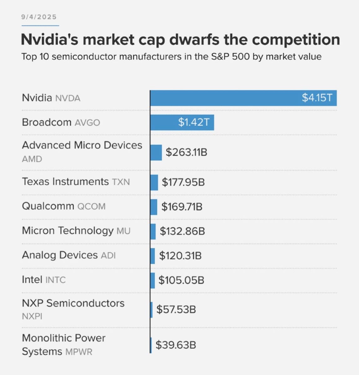


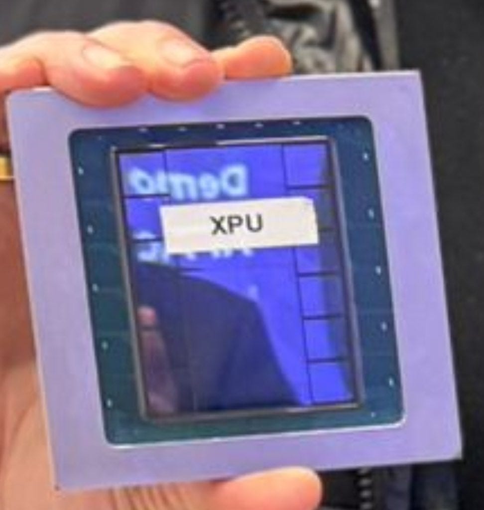
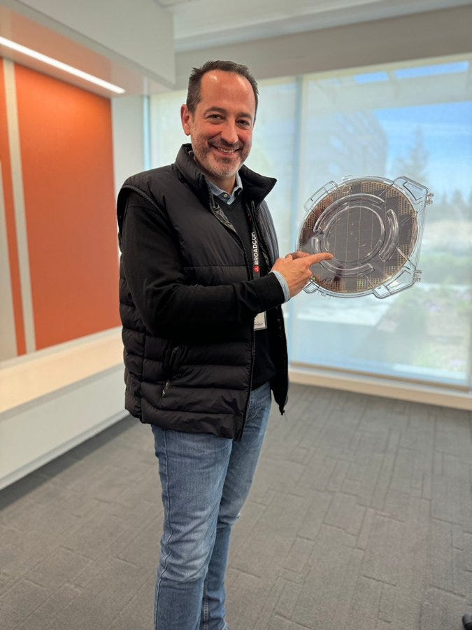
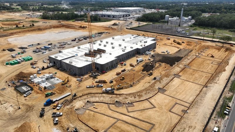
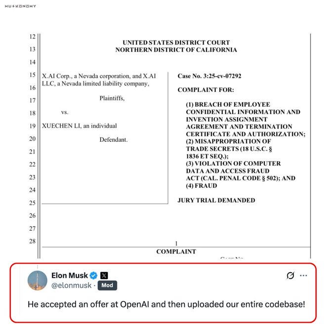


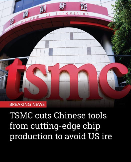

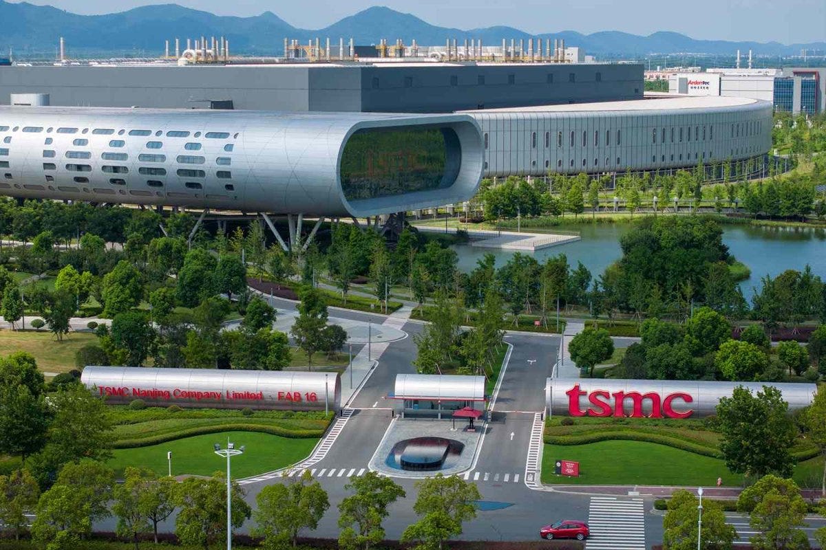
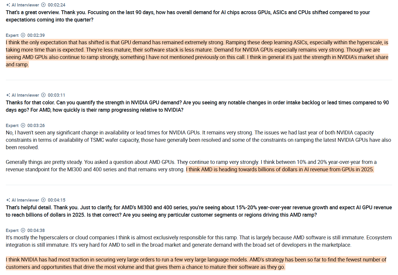
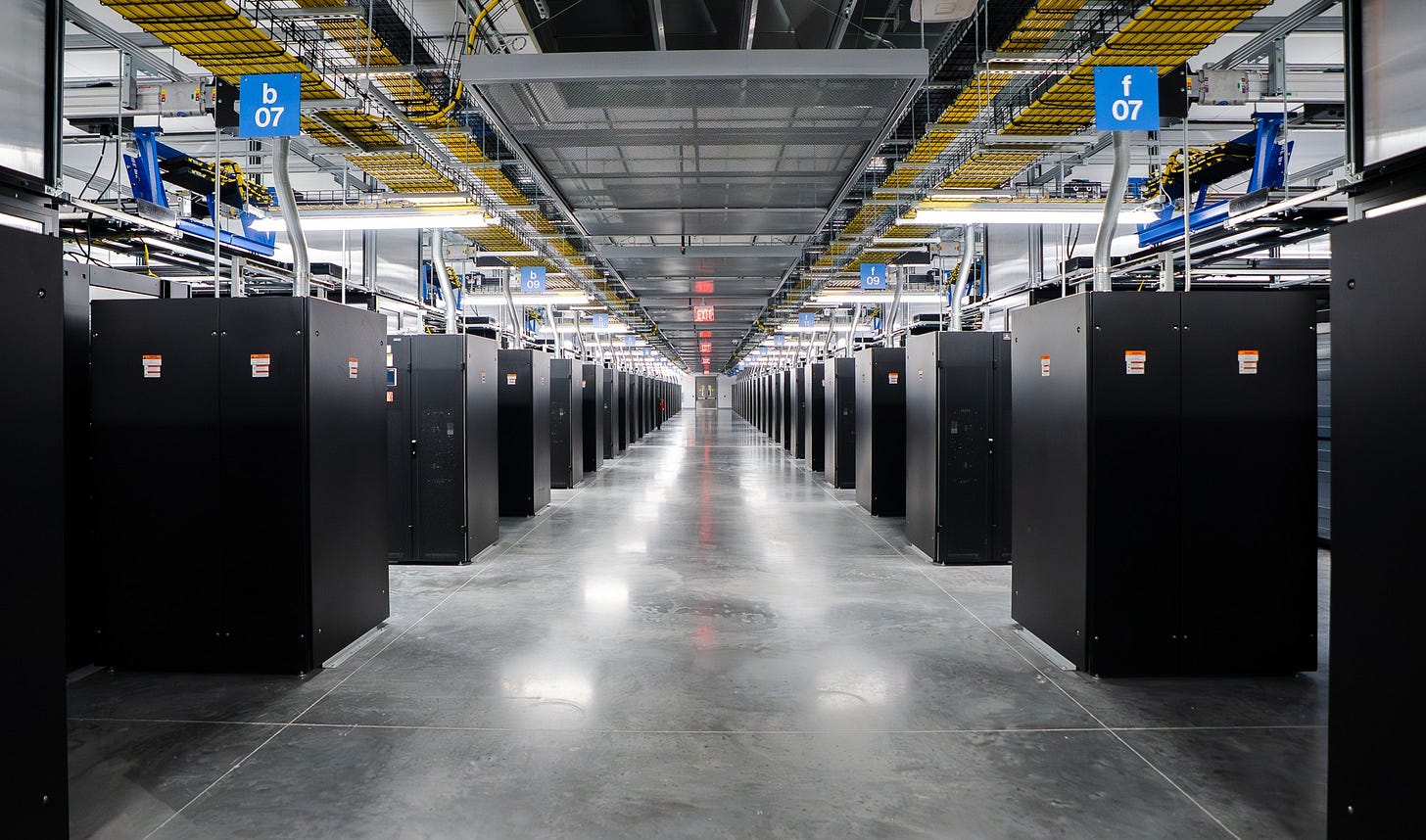
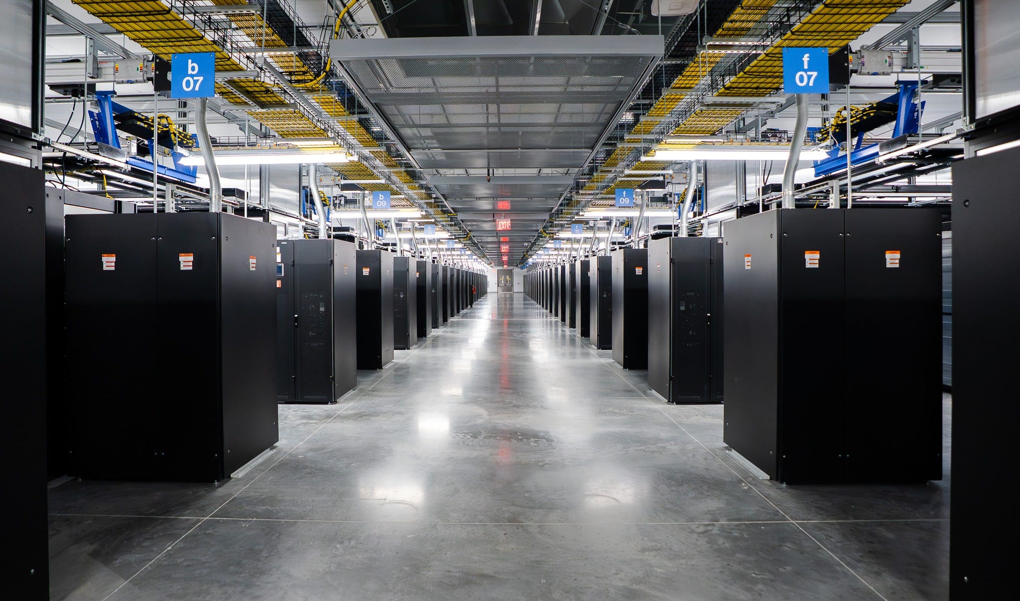
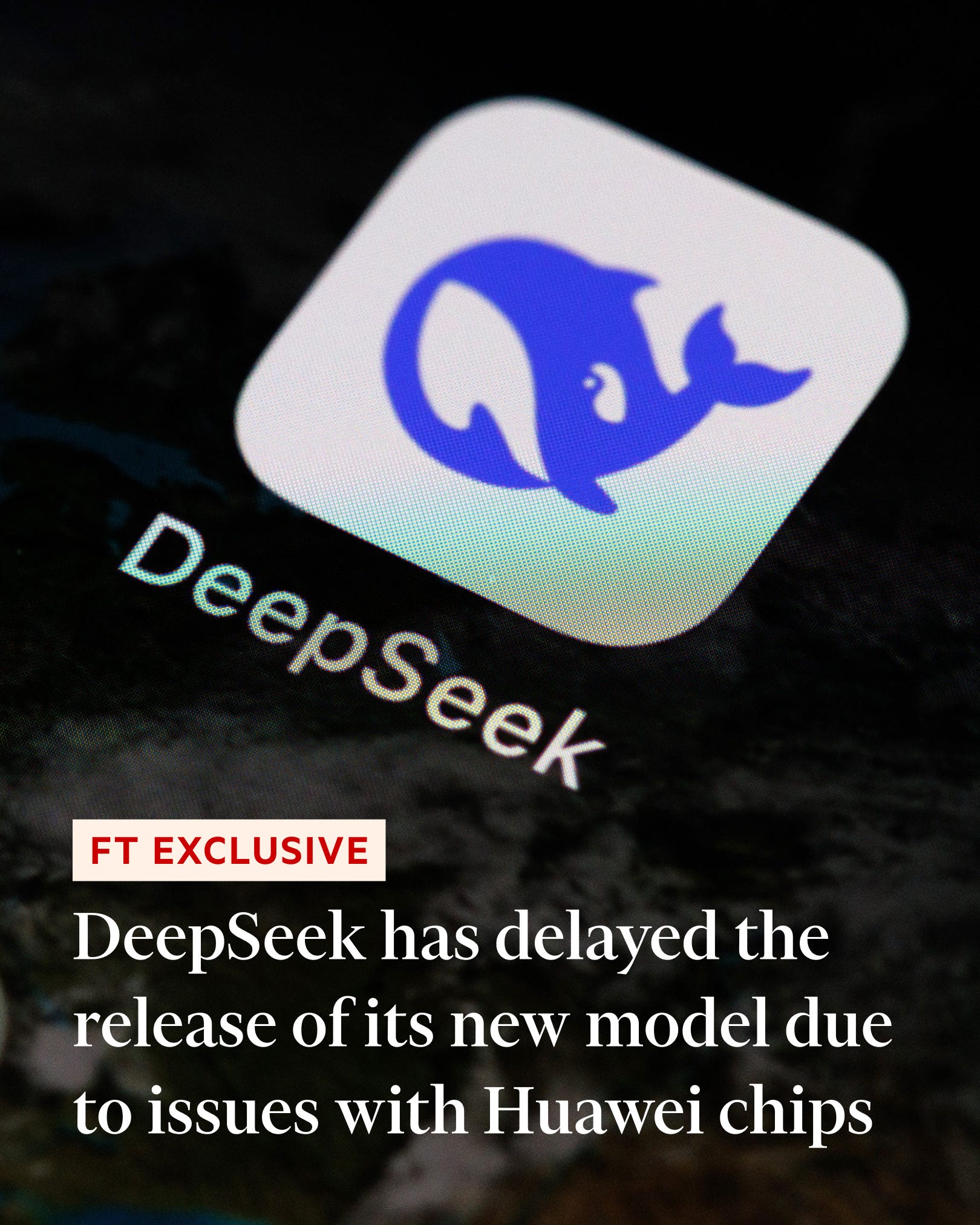


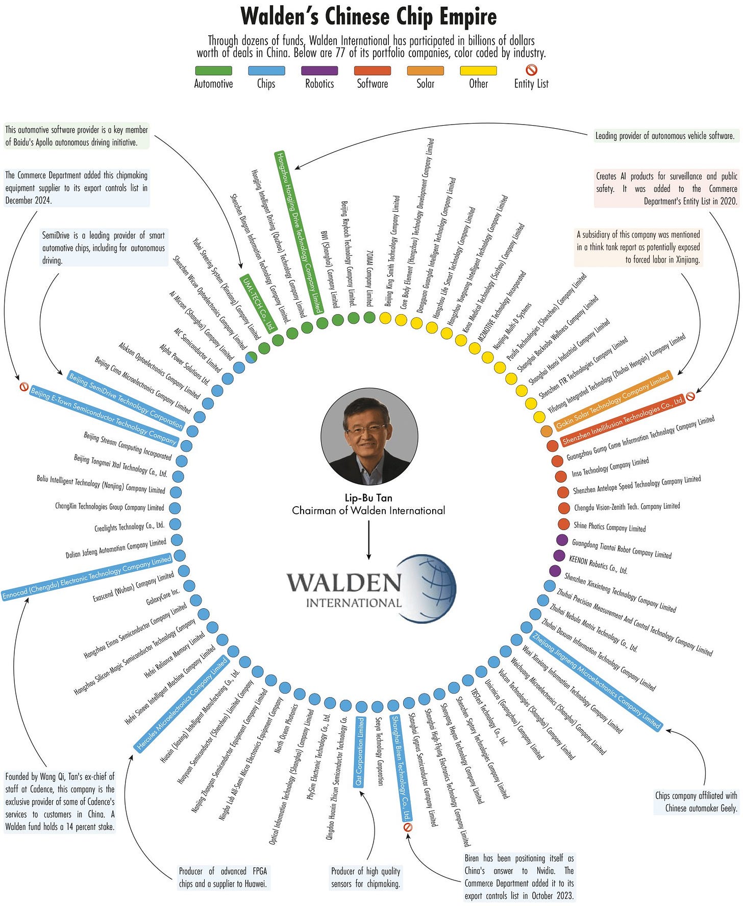

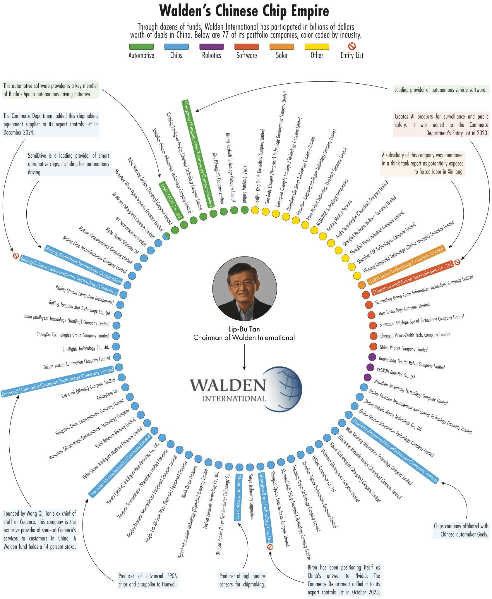
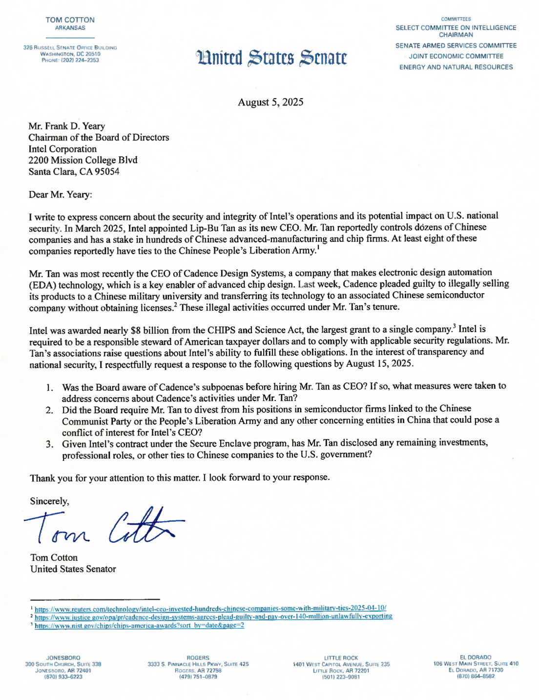

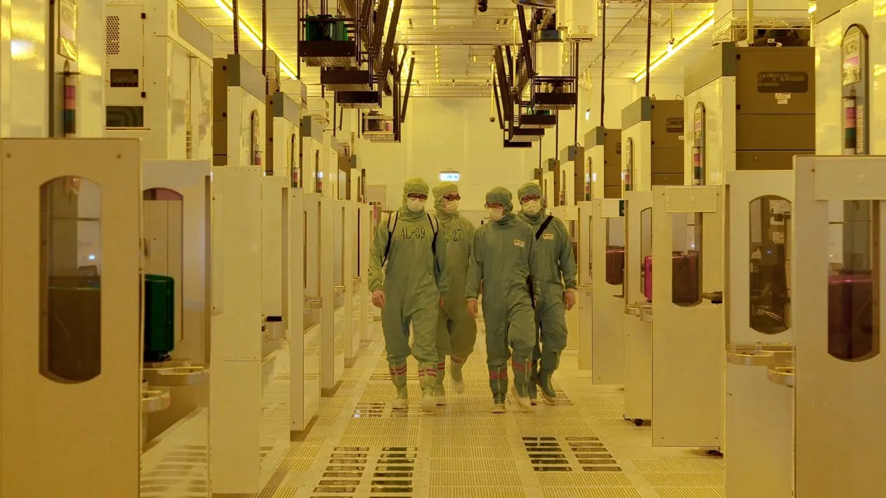
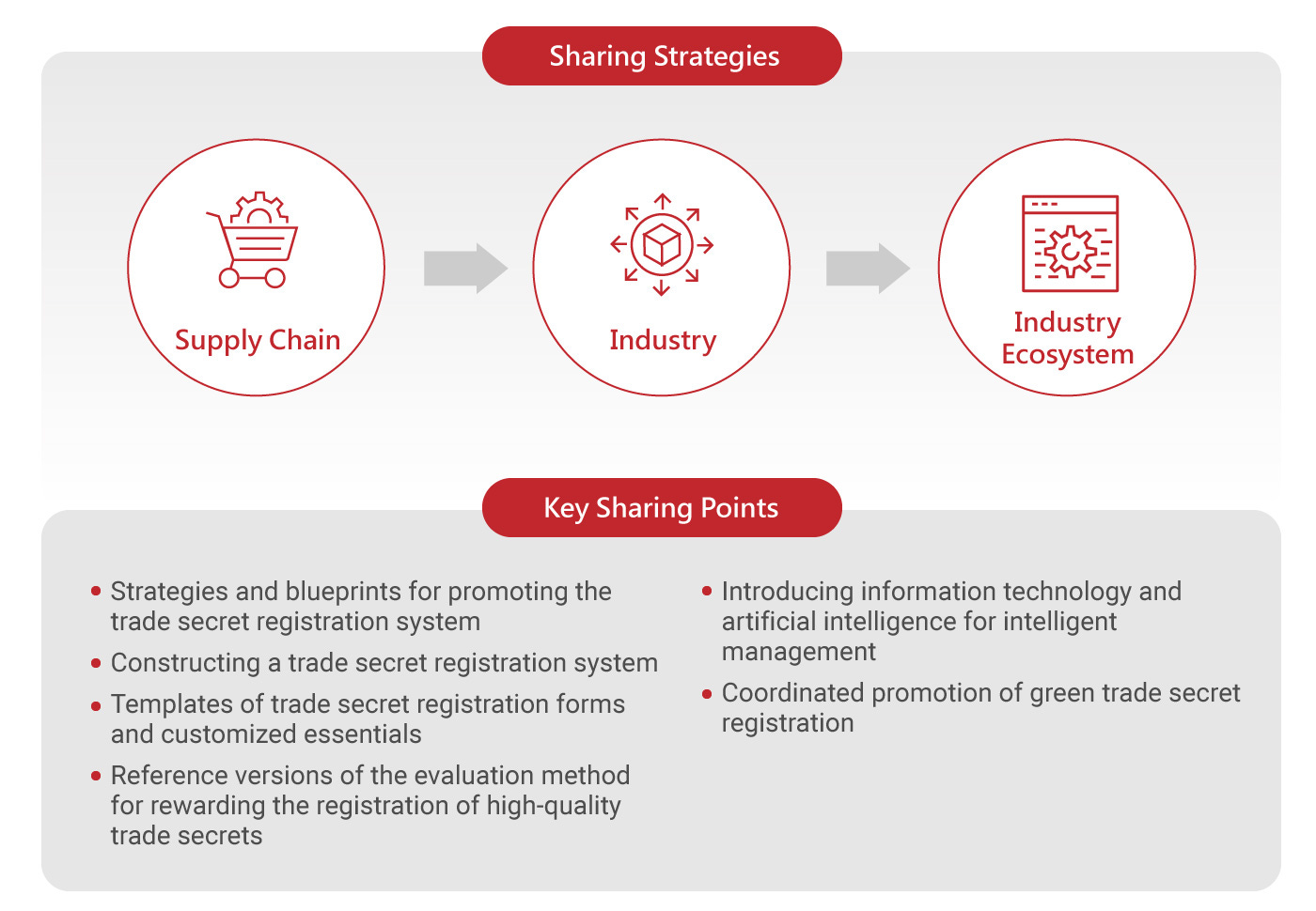

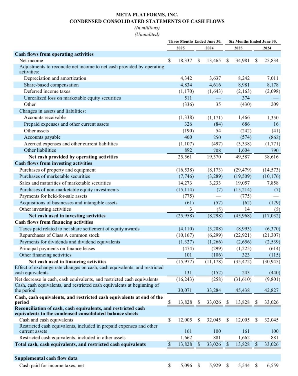


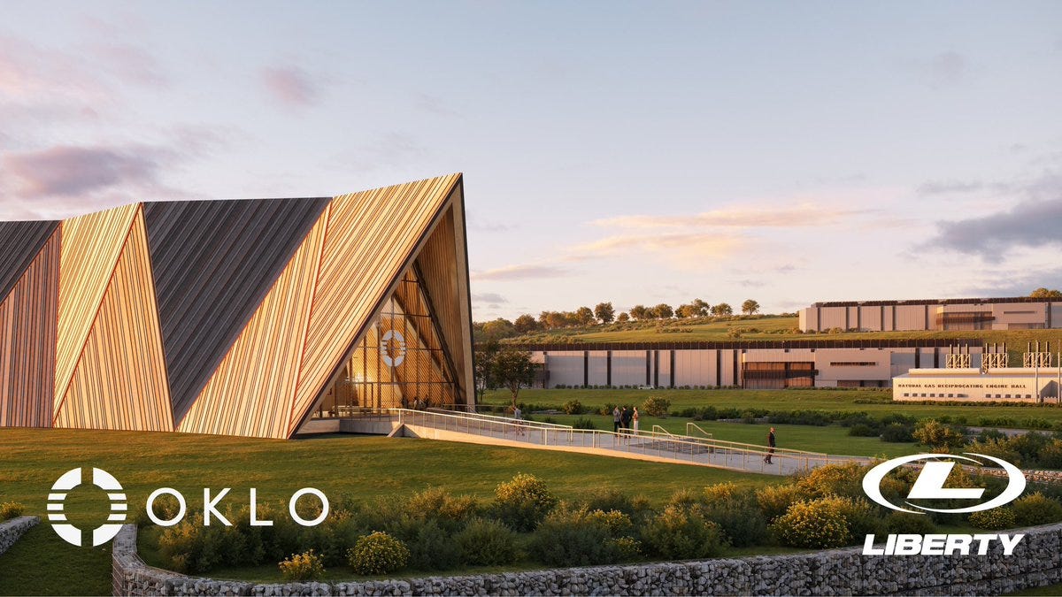
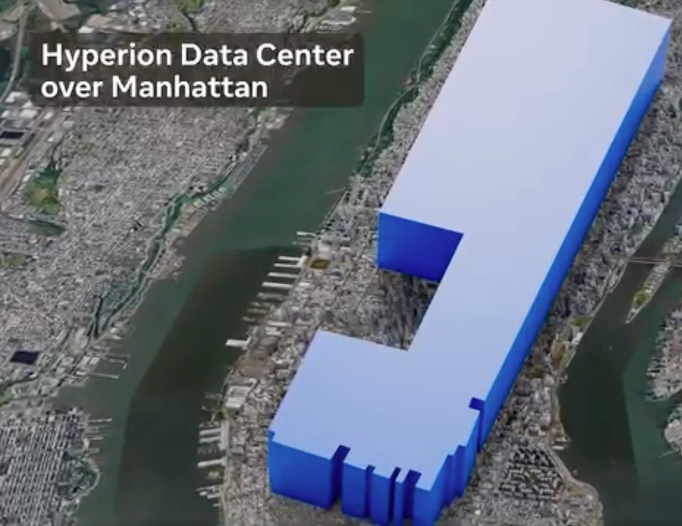


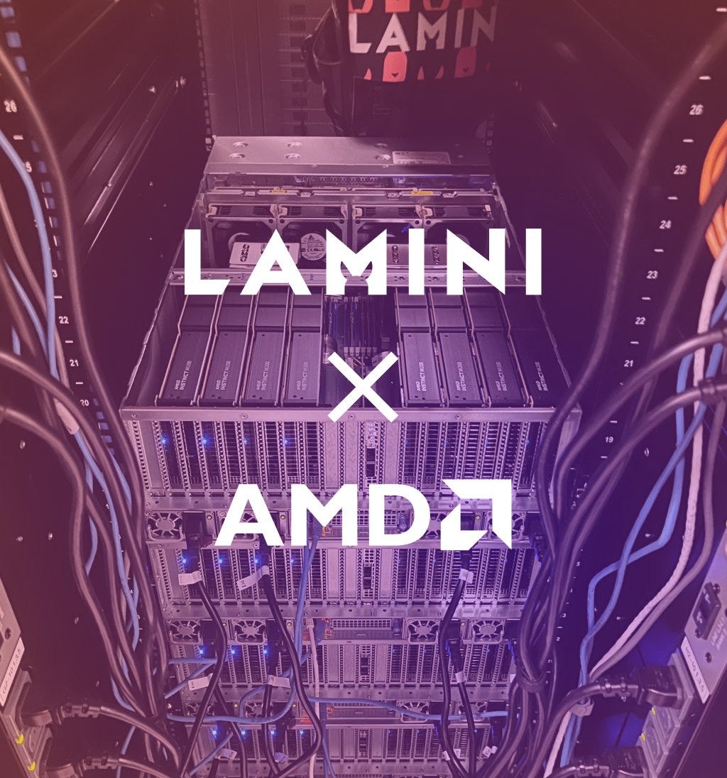


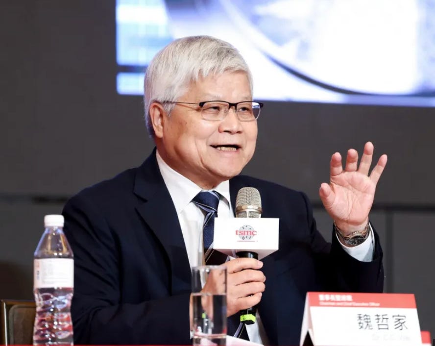


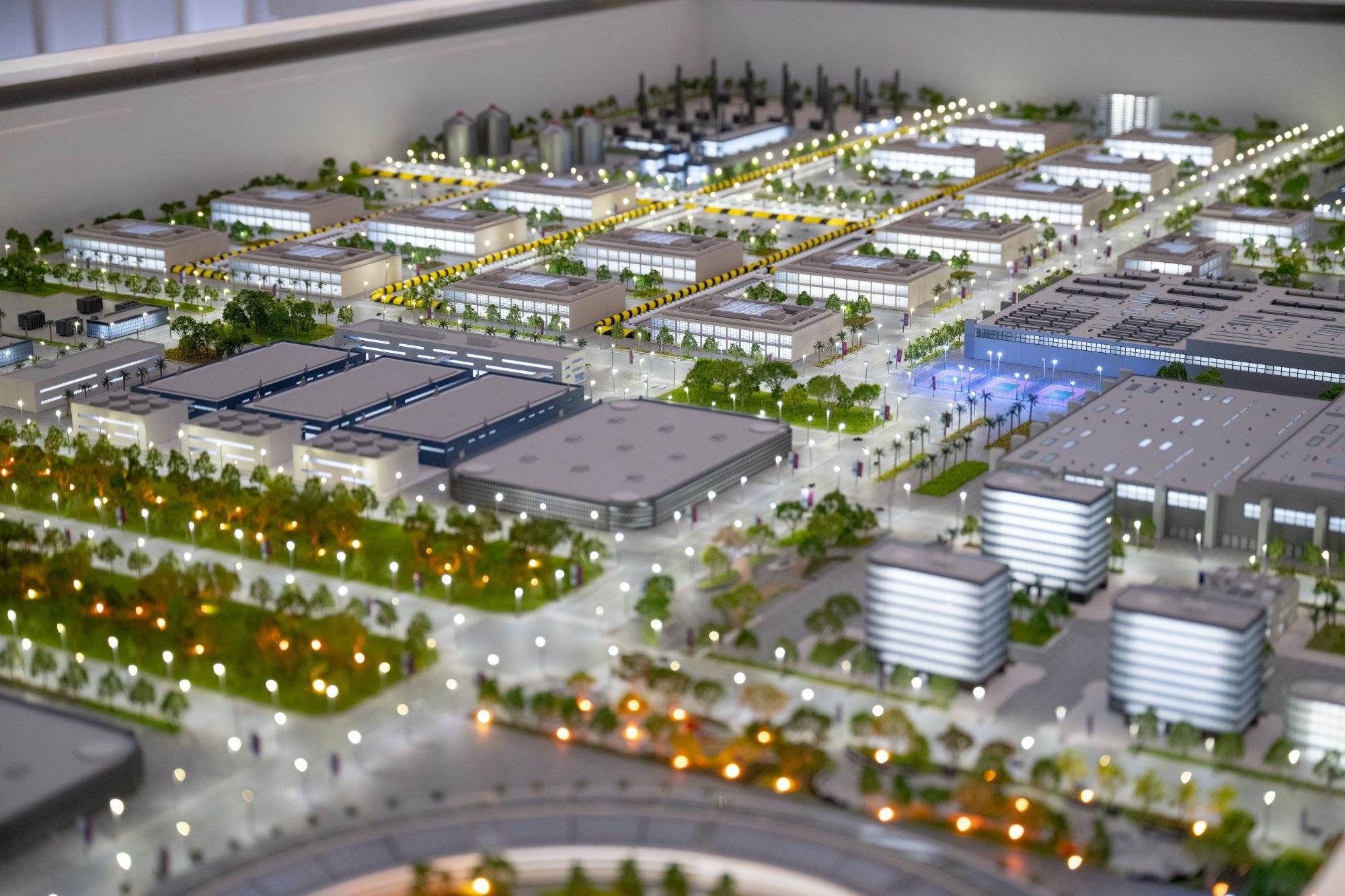

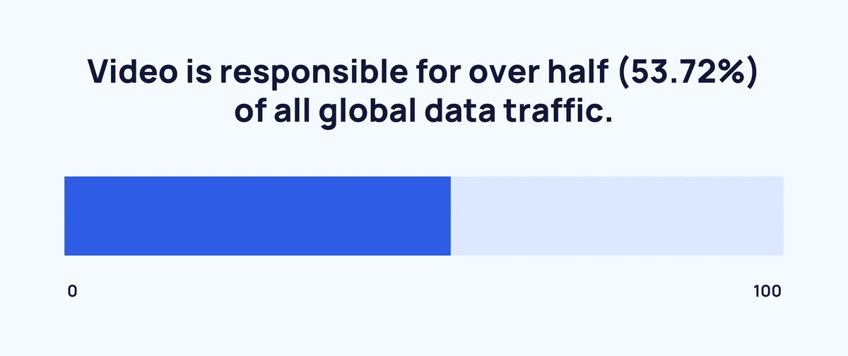

![Researchers from Shanghai-based Fudan University, who have developed a picosecond-level flash memory device, work in their lab. [Photo by Gao Erqiang/chinadaily.com.cn]](https://substackcdn.com/image/fetch/$s_!i4m8!,f_auto,q_auto:good,fl_progressive:steep/https%3A%2F%2Fsubstack-post-media.s3.amazonaws.com%2Fpublic%2Fimages%2F8b7f251f-2904-4d43-a2c1-36ba95046d89_799x533.jpeg "Researchers from Shanghai-based Fudan University, who have developed a picosecond-level flash memory device, work in their lab. [Photo by Gao Erqiang/chinadaily.com.cn]")


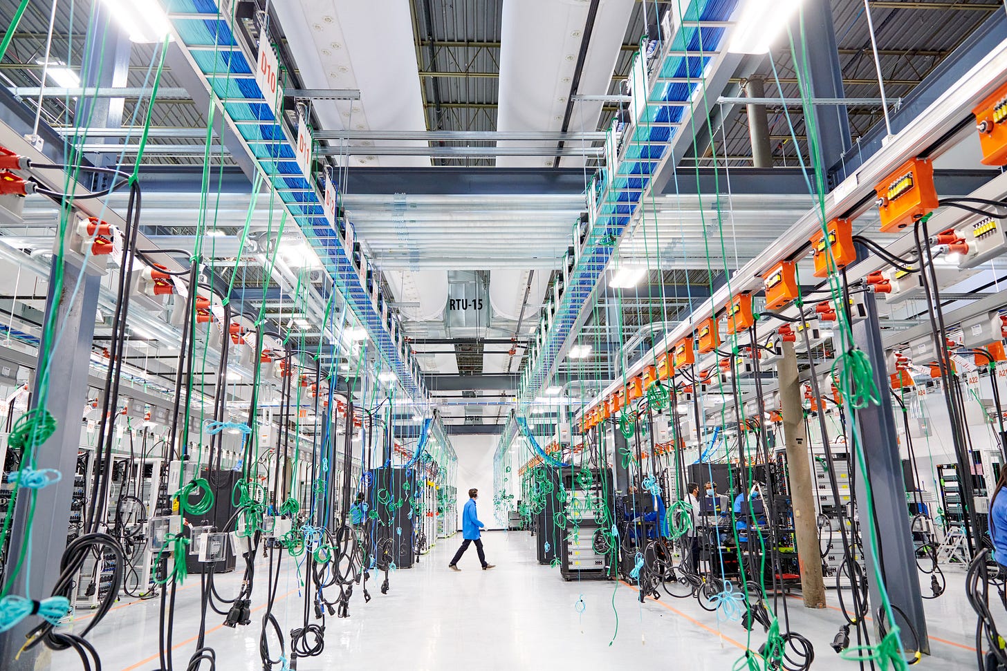

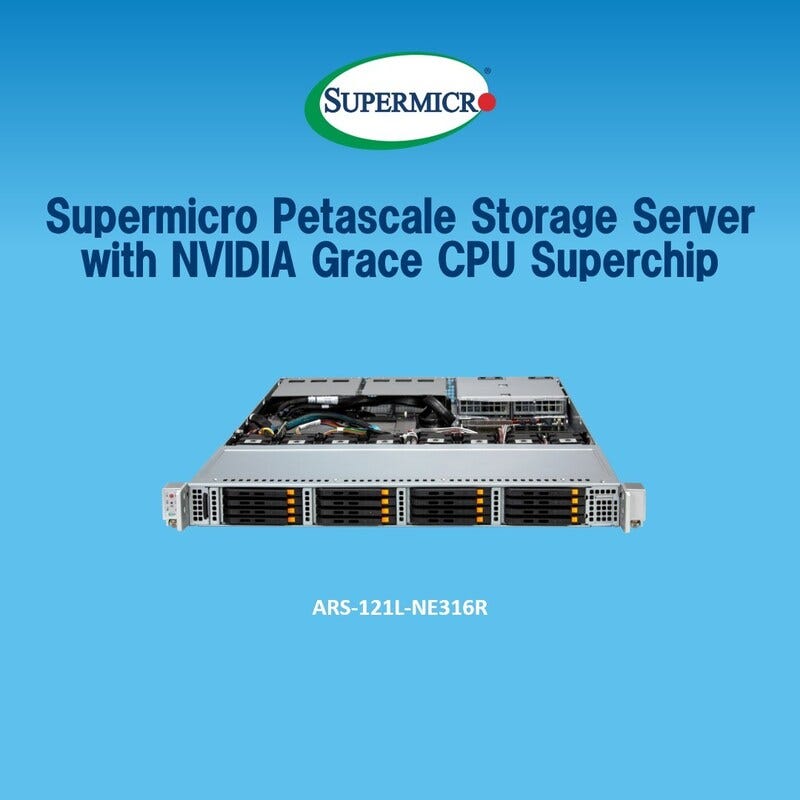
, the largest private owner of power generation and renewables in the USA, have entered into an agreement to establish a 50-50 partnership in new build power generation and energy infrastructure.")


 Notice Regarding the Transfer of Fixed Assets Sharp Corporation (hereinafter \"Sharp\") hereby announces that Sharp have entered into the sale and purchase agreement with SoftBank Corp. (hereinafter \"Softbank\") regarding the fixed assets (land, buildings etc.) owned by Sharp and its subsidiary, and have transferred (delivered) the relevant properties to Softbank today. This is related to the \"Notice Regarding the Transfer of Fixed Assets\" dated December 20, 2024, in which Sharp announced the board resolution to transfer the fixed assets (land, buildings etc.) owned by Sharp and its subsidiary to Softbank. 1. Reason for the Transfer Please refer to \"Notice Regarding the Transfer of Fixed Assets\" dated December 20, 2024. 2. Details of the Assets to be Transferred 3. Outline of the Counterparty Please refer to \"Notice Regarding the Transfer of Fixed Assets\" dated December 20, 2024. 4. Schedule Contract and Transfer Date: March 14, 2025 5. Future Prospects As a result of the above transfer of fixed assets, Sharp expect to record a gain on sale of non-current assets of 75,424 million yen in the financial results for the fiscal year ending March 31, 2025. Regarding the consolidated financial results for the fiscal year ending March 31, 2025, with the impact of this asset transfer transaction, Sharp expects that the profit attributable to owners of parent will exceed the originally announced forecast of 5 billion yen. However, as it is difficult to make a reasonable estimate on various expenses related to other structural reform to aim for a business growth in fiscal 2025 and beyond, Sharp continues to state that its profit attributable to owners of parent remains undetermined.")
 Notice Regarding the Transfer of Fixed Assets Sharp Corporation (hereinafter \"Sharp\") hereby announces that Sharp have entered into the sale and purchase agreement with SoftBank Corp. (hereinafter \"Softbank\") regarding the fixed assets (land, buildings etc.) owned by Sharp and its subsidiary, and have transferred (delivered) the relevant properties to Softbank today. This is related to the \"Notice Regarding the Transfer of Fixed Assets\" dated December 20, 2024, in which Sharp announced the board resolution to transfer the fixed assets (land, buildings etc.) owned by Sharp and its subsidiary to Softbank. 1. Reason for the Transfer Please refer to \"Notice Regarding the Transfer of Fixed Assets\" dated December 20, 2024. 2. Details of the Assets to be Transferred 3. Outline of the Counterparty Please refer to \"Notice Regarding the Transfer of Fixed Assets\" dated December 20, 2024. 4. Schedule Contract and Transfer Date: March 14, 2025 5. Future Prospects As a result of the above transfer of fixed assets, Sharp expect to record a gain on sale of non-current assets of 75,424 million yen in the financial results for the fiscal year ending March 31, 2025. Regarding the consolidated financial results for the fiscal year ending March 31, 2025, with the impact of this asset transfer transaction, Sharp expects that the profit attributable to owners of parent will exceed the originally announced forecast of 5 billion yen. However, as it is difficult to make a reasonable estimate on various expenses related to other structural reform to aim for a business growth in fiscal 2025 and beyond, Sharp continues to state that its profit attributable to owners of parent remains undetermined.")
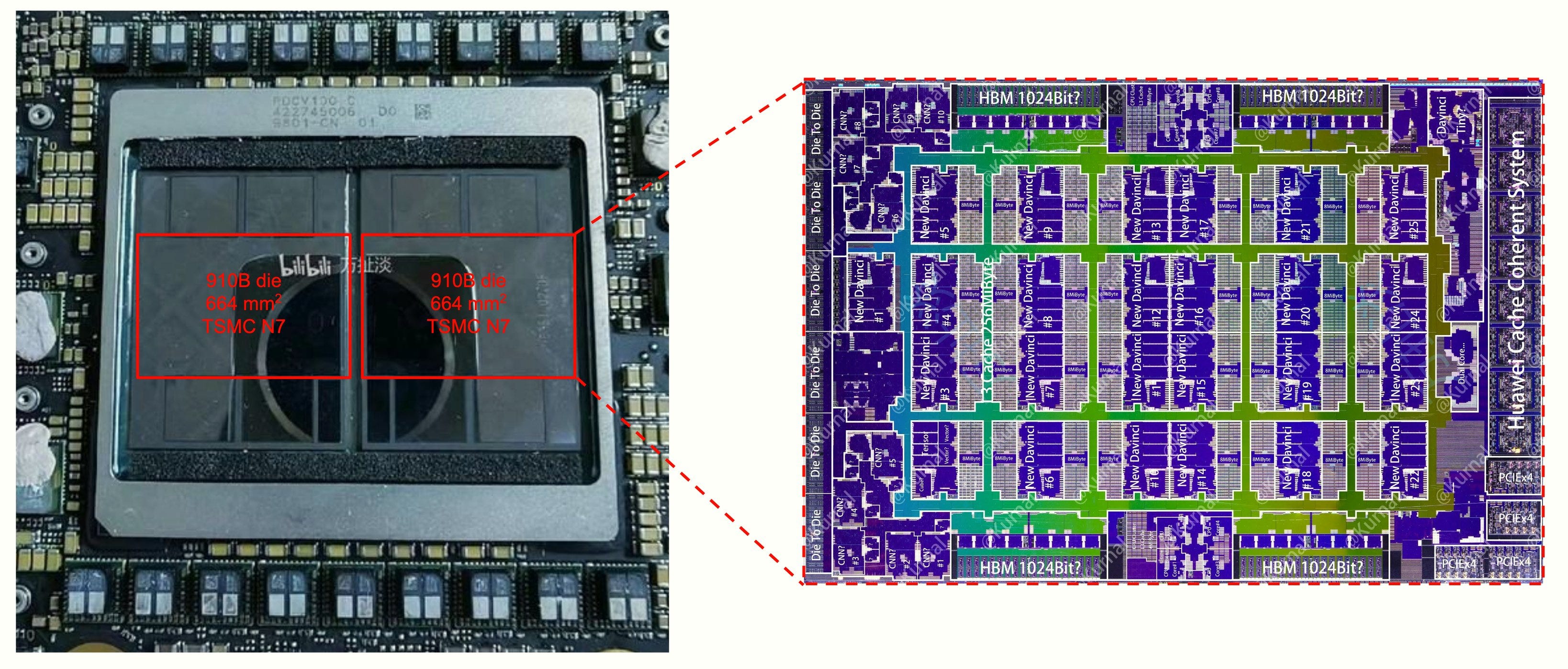

, that would imply the production of millions of Ascend 910C chips annually.")


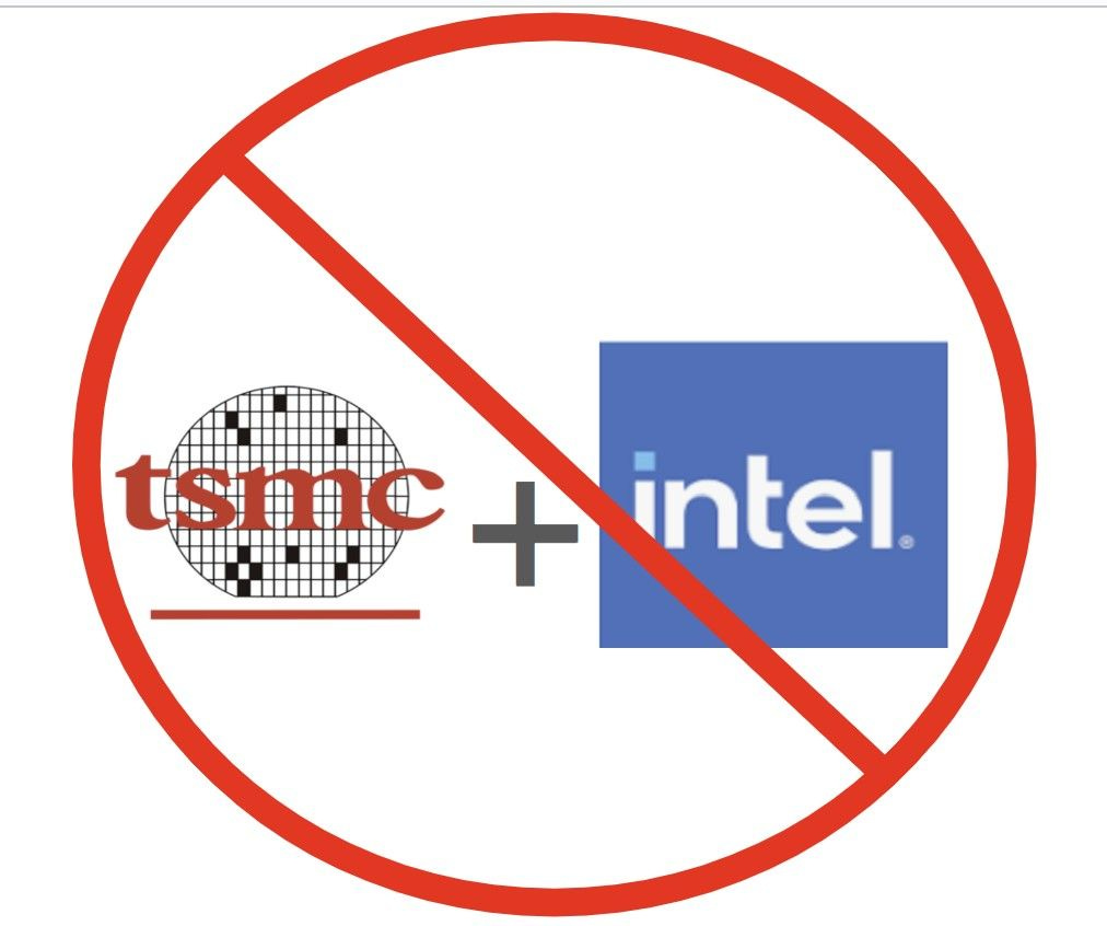
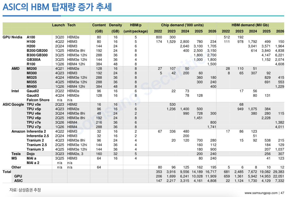


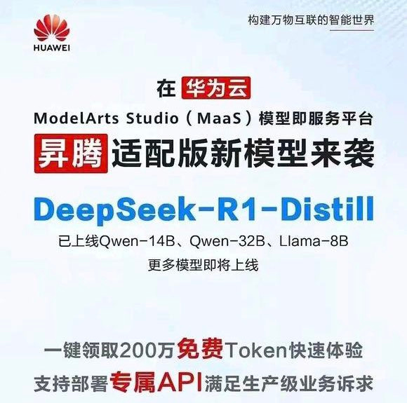


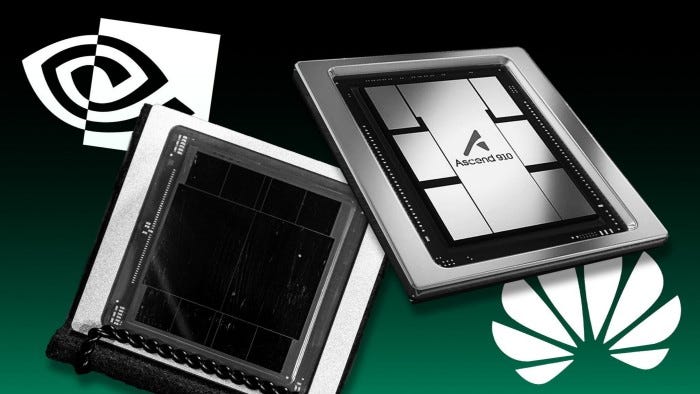


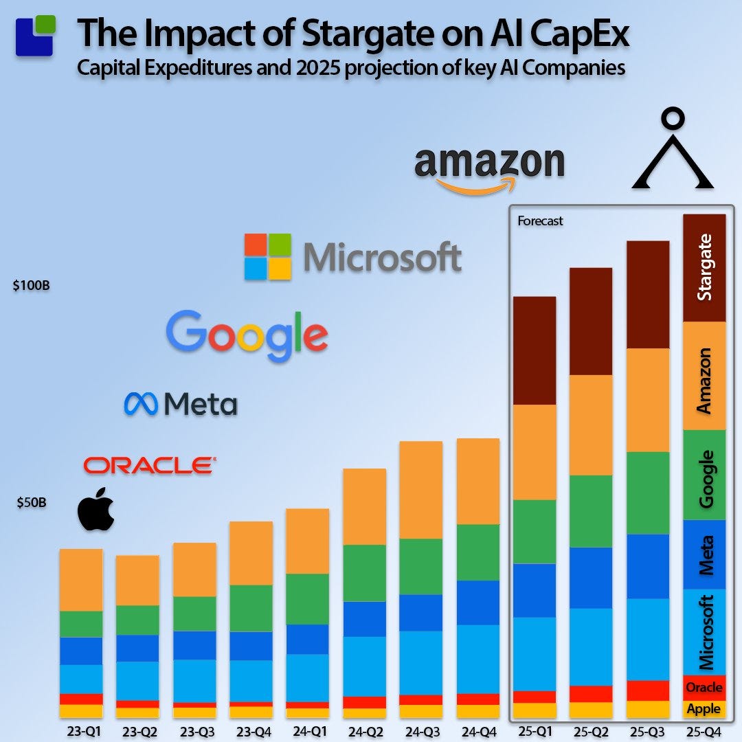


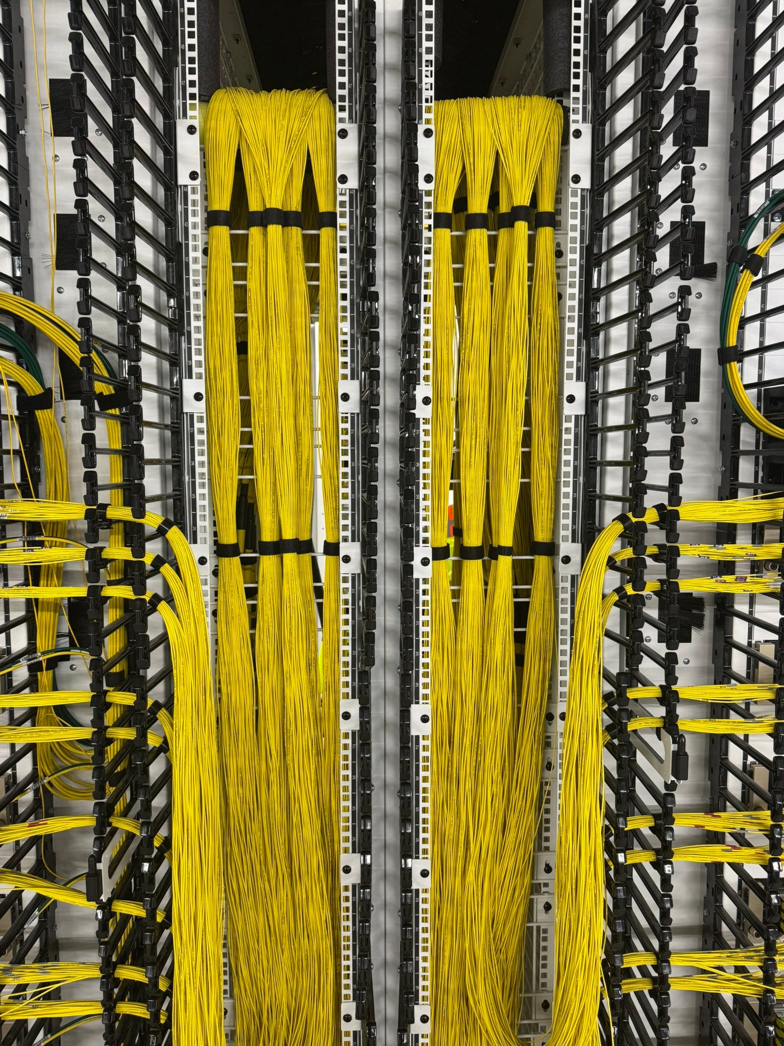
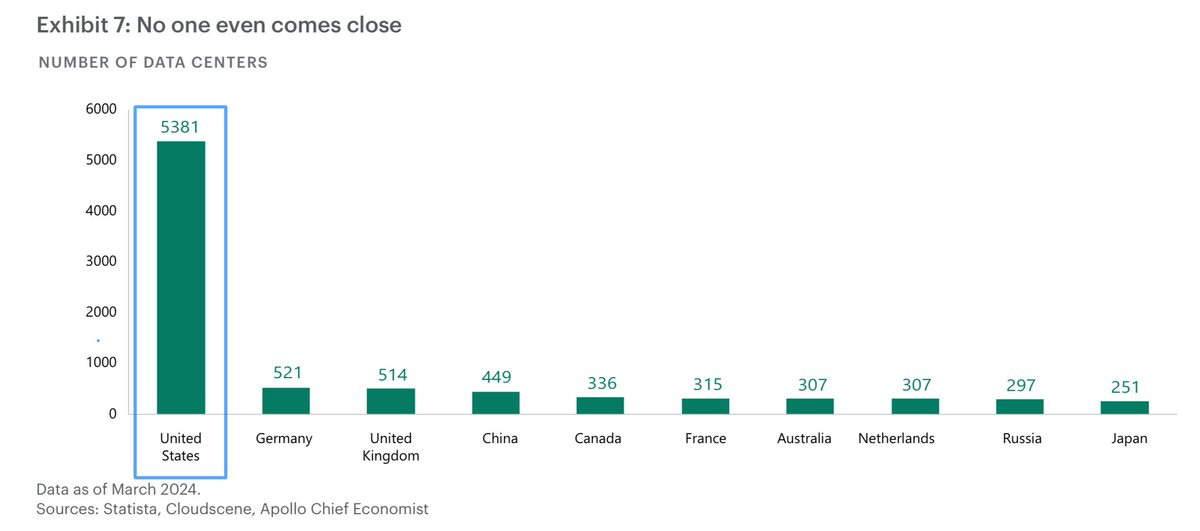

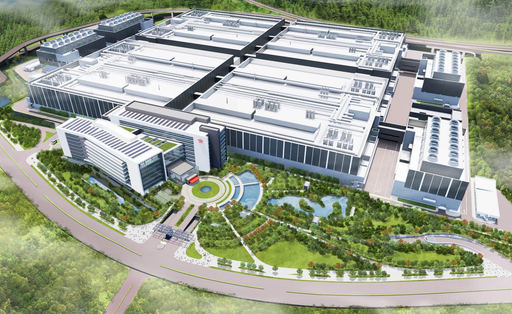

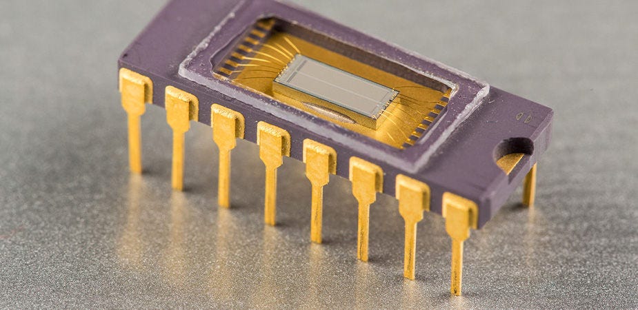
 or low-level (TT-Metalium™) development.")
 or low-level (TT-Metalium™) development.")